
Data Sheet

www.onsemi.com
13
FAN7930C — Critical Conduction Mode PFC Controller
I
SW
V
AUX
& V
ZCD
V
ACIN
I
MOSFET
I
DIODE
V
AUX
V
ZCD
t
6.2V
0.65V
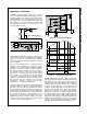
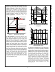
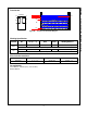
Figure 28. Auxiliary Voltage Depends on
MOSFET Switching
The auxiliary w inding voltage is used to check the boost
inductor current zero instance. When boost inductor
current becomes zero, there is a resonance betw een
boost inductor and all capacitors at the MOSFET drain
pin: including C
OSS
of the MOSFET; an external
capacitor at the D-S pin to reduce the voltage rising and
falling slope of the MOSFET; a parasitic capacitor at
inductor; and so on to improve performance. Resonated
voltage is reflected to the auxiliary w inding and can be
used for detecting zero current of boost inductor and
valley position of MOSFET voltage stress. For valley
detection, a minor delay by the resistor and capacitor is
needed. A capacitor increases the noise immunity at the
ZCD pin. If ZCD voltage is higher than 1.5 V, an internal
ZCD comparator output becomes HIGH and LOW w hen
the ZCD goes below 1.4 V. At the falling edge of
comparator output, internal logic turns on the MOSFET
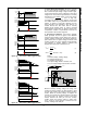
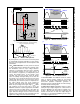
V
IN
V
OUT
PFC
- V
IN
1.5V
150ns Delay
1.4V
ON
ON
V
OUT
PFC
- V
IN
I
MOSFET
I
DIODE
V
ZCD
t
I
INDUCTOR
V
DS
MOSFET gate
Figure 29. Auxiliary Voltage Threshold
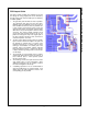
When no ZCD signal is available, the PFC controller
cannot turn on the MOSFET, so the controller checks
every switching off time and forces MOSFET turn on
when the off time is longer than 150 μs. This restart
timer triggers MOSFET turn-on at startup and may be
used at the input voltage zero-cross period.
V
OUT
V
IN
V
CC
t
RESTART
MOSFET gate
ZCD
after COMPARATOR
t
s150
Figure 30. Restart Timer at Startup
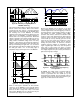
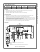
Because the MOSFET turn-on depends on the ZCD
input, sw itching frequency may increase to higher than
several megahertz due to the mis-triggering or noise on
the nearby ZCD pin. If the sw itching frequency is higher
than needed for critical conduction mode (CRM),
operation mode shifts to continuous conduction mode
(CCM). In CCM, unlike CRM w here the boost inductor
current is reset to zero at the next sw itch on; inductor
current builds up at every sw itching cycle and can be
raised to very high current that exceeds the current
rating of the pow er sw itch or diode. This can seriously
damage the pow er sw itch. To avoid this, maximum
sw itching frequency limitation is embedded. If ZCD
signal is applied again w ithin 3.3 μs after the previous
rising edge of gate signal, this signal is ignored
internally and FA N7930C w aits for another ZCD signal.
This slightly degrades the pow er factor performance at
light load and high input voltage.
ZCD
after COMPARATOR
MOSFET Gate
Max. f
SW
Limit
Inhibit Region
Error occurs!
Ignores ZCD noise
t
Figure 31. Maximum Switching Frequency
Limit Operation
6. Control: The scaled output is compared w ith the
internal reference voltage and sinking or sourcing
current is generated from the COMP pin by the
transconductance amplifier. The error amplifier output is
compared w ith the internal saw tooth w aveform to give
proper turn-on time based on the controller.