
Data Sheet

www.onsemi.com
12
FAN7930C — Critical Conduction Mode PFC Controller
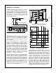
PFC operation
V
CC
V
START
V
STOP
5V
V
INV
(=V
PFCOUT
)
2.240V
2.051V
V
RDY
2.500V
t
PFC operation
V
CC
V
START
V
STOP
5V
V
INV
(=V
PFCOUT
)
2.240V
2.051V
V
RDY
2.500V
t
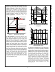
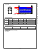
Figure 25. Two Cases of RDY Triggered HIGH
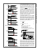
PFC operation
V
CC
V
START
V
STOP
5V
V
INV
(=V
PFCOUT
)
2.240V
2.051V
V
RDY
2.500V
t
PFC operation
V
CC
V
START
V
STOP
5V
V
INV
(=V
PFCOUT
)
2.240V
2.051V
V
RDY
2.500V
t
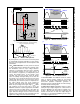
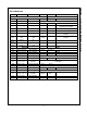
Figure 26. Two Cases of RDY Triggered LOW
4. Control Range Compensation: On time is controlled
by the output voltage compensator w ith FAN7930C.
Due to this w hen input voltage is high and load is light,
control range becomes narrow compared to w hen input
voltage is low . That control range decrease is inversely
proportional to the double square of the input voltage
(
). Thus at high line,
unw anted burst operation easily happens at light load
and audible noise may be generated from the boost
inductor or inductor at input filter. Different from the
other converters, burst operation in PFC block is not
needed because the PFC block itself is normally
disabled during standby mode. To reduce unw anted
burst operation at light load, an internal control range
compensation function is implemented and show s no
burst operation until 5% load at high line.
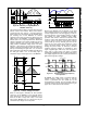
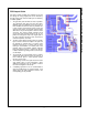
5. Zero-Current Detection: Zero-current detection
(ZCD) generates the turn-on signal of the MOSFET
when the boost inductor current reaches zero using an
auxiliary w inding coupled w ith the inductor. When the
pow er sw itch turns on, negative voltage is induced at the
auxiliary w inding due to the opposite w inding direction
(see Equation 1). Positive voltage is induced (see
Equation 2) w hen the pow er switch turns off.
AC
IND
AUX
AUX
V
T
T
V
(1)
ACPFCOUT
IND
AUX
AUX
VV
T
T
V
(2)
w here:
V
AUX
is the auxiliary w inding voltage;
T
IND
is boost inductor turns;
T
IND
auxiliary w inding turns;
V
AC
is input voltage for PFC converter; and
V
OUT_PFC
is output voltage from the PFC converter.
PFC Inductor
Aux Winding
V
IN
PFC
V
OUT
PFC
ZCD
V
TH(ZCD)
+
-
V
CC
THD optimized
Sawtooth
Generator
Restart
Timer
gate
driver
R
ZCD
C
ZCD
Negative Clamp
Circuit
Positive Clamp
Circuit
5
S
Q
R
Q
f
MAX
limit
optional
Figure 27. Circuit Near ZCD
Because auxiliary w inding voltage can sw ing from
negative to positive voltage, the internal block in ZCD
pin has both positive and negative voltage c lamping
circuits. When the auxiliary voltage is negative, an
internal circuit clamps the negative voltage at the ZCD
pin around 0.65 V by sourcing current to the serial
resistor betw een the ZCD pin and the auxiliary
w inding. When the auxiliary voltage is higher than
6.5 V, current is sinked through a resistor from the
auxiliary w inding to the ZCD pin.