
Data Sheet

www.onsemi.com
11
FAN7930C — Critical Conduction Mode PFC Controller
Applications Information
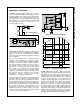
1. Startup: Normally, supply voltage (V
CC
) of a PFC
block is fed from the additional pow er supply, w hich can
be called standby pow er. Without this standby pow er,
auxiliary w inding for zero current detection can be used
as a supply source. Once the supply voltage of the PFC
block exceeds 12 V, internal operation is enabled until
the voltage drops to 8.5 V. If V
CC
exceeds V
Z
, 20 mA
current is sinking from V
CC
.
V
CC
V
Z
+
-
V
TH(S/S)
12
8.5
V
CC
’
2.5V
REF
Internal
Bias
V
BIAS
V
REF
reset
H:open
20mA
PFC Inductor
Aux. Winding
V
IN
PFC
V
OUT
PFC
External V
CC
circuit
when no standby power exists
8
Figure 22. Startup Circuit
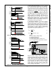
2. INV Block: Scaled-dow n voltage from the output is
the input for the INV pin. Many functions are embedded
based on the INV pin: transconductance amplifier,
output OV P comparator, disable comparator, and output
UVLO comparator.
For the output voltage control, a transconductance
amplifier is used instead of the conventional voltage
amplifier. The transconductance amplifier (voltage-
controlled current source) aids the implementation of
the OV P and disable functions. The output current of
the amplifier changes according to the voltage
difference of the inverting and non-inverting input of
the amplifier. To cancel dow n the line input voltage
effect on pow er factor correction, the effective control
response of the PFC block should be slow er than the
line frequency and this conflicts w ith the transient
response of controller. Tw o-pole one-zero type
compensation can meet both requirements.
The OV P comparator shuts dow n the output drive block
when the voltage of the INV pin is higher than 2.675 V
and there is 0.175 V hysteresis. The disable comparator
disables operation w hen the voltage of the inverting input
is low er than 0.35 V and there is 100 mV hysteresis. An
external small-signal MOSFET can be used to disable the
IC, as show n in Figure 23. The IC operating current
decreases to reduce pow er consumption if the IC is
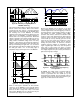
disabled. Figure 24 is the timing chart of the internal
circuit near the INV pin w hen rated PFC output voltage
is 390 V
DC
and V
CC
supply voltage is 15 V.
+
-
+
-
+
-
V
OUT
PFC
+
-
2.5V
0.45V/0.35V
INV open
2.675V/2.5V
OVP
2.240V/2.051V
UVLO
2.240
2.051
high
V
CC
’
disable
1
INV
3
COMP
2
RDY
0.45
0.35
disable
2.675
2.5
disable
Figure 23. Circuit Around INV Pin
390Vdc
2.50V
2.65V
0.45V
Current sourcing Current sourcing
I sinking
0.35V
2.051V
2.24V
2.50V
2.0V
349V
413V
390V
320V
70V
55V
V
OUT
PFC
V
INV
V
CC
I
OUT
COMP
Disable
V
RDY
OVP
t
Voltage is decided by pull-up voltage.
Vcc<2V, internal logic is not alive.
- RDY pin is floating, so pull up voltage is shown.
- Internal signals are unknown.
15V
Figure 24. Timing Chart for INV Block
3. RDY Output: When the INV voltage is higher than
2.24 V, RDY output is triggered HIGH and lasts until the
INV voltage is low er than 2.051 V. When input AC
voltage is quite high, for example 240 V
AC
, PFC output
voltage is alw ays higher than RDY threshold, regardless
of boost converter operation. In this case, the INV
voltage is already higher than 2.24 V before PFC V
CC
touches V
START
; how ever, RDY output is not triggered to
HIGH until V
CC
touches V
START
. After boost converter
operation stops, RDY is not pulled LOW because the
INV voltage is higher than the RDY threshold. When V
CC
of the PFC drops below 5 V, RDY is pulled LOW even
though PFC output voltage is higher than threshold. The
RDY pin output is open drain, so needs an external pull-
up resistor to supply the proper pow er source. The RDY
pin output remains floating until V
CC
is higher than 2 V.