
Data Sheet

© 2008 Fairchild Semiconductor Corporation www.fairchildsemi.com
FAN7888 • Rev.1.5 5
FAN7888 — 3 Half-Bridge Gate-Drive IC
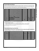
Electrical Characteristics
V
BIAS
(V
DD
, V
BS1,2,3
)=15.0 V, T
A
=25C, unless otherwise specified. The V
IN
and I
IN
parameters are referenced to
GND. The V
O
and I
O
parameters are referenced to GND and V
S1,2,3
and are applicable to the respective outputs
LO1,2,3 and HO1,2,3.
Note:
4. This parameter is guaranteed by design.
Symbol Characteristics Condition Min. Typ. Max. Unit
LOW-SIDE POWER SUPPLY SECTION
I
QDD
Quiescent V
DD
Supply Current V
LIN1,2,3
=0 V or 5 V 160 350 µA
I
PDD1,2,3
Operating V
DD
Supply Current for each
Channel
f
LIN1,2,3
=20 kHz, rms Value 500 900 µA
V
DDUV+
V
DD
Supply Under-Voltage Positive-Going
Threshold
V
DD
=Sweep, V
BS
=15 V 7.2 8.2 9.0 V
V
DDUV-
V
DD
Supply Under-Voltage Negative-Going
Threshold
V
DD
=Sweep, V
BS
=15 V 6.8 7.8 8.5 V
V
DDHYS
V
DD
Supply Under-Voltage Lockout
Hysteresis
V
DD
=Sweep, V
BS
=15 V 0.4 V
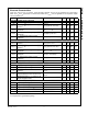
BOOTSTRAPPED POWER SUPPLY SECTION
I
QBS1,2,3
Quiescent V
BS
Supply Current for each
Channel
V
HIN1,2,3
=0 V or 5 V 50 120 µA
I
PBS1,2,3
Operating V
BS
Supply Current for each
Channel
f
HIN1,2,3
=20 kHz, rms Value 400 800 µA
V
BSUV+
V
BS
Supply Under-Voltage Positive-going
Threshold
V
DD
=15 V, V
BS
=Sweep 7.2 8.2 9.0 V
V
BSUV-
V
BS
Supply Under-Voltage Negative-going
Threshold
V
DD
=15 V, V
BS
=Sweep 6.8 7.8 8.5 V
V
BSHYS
V
BS
Supply Under-Voltage Lockout
Hysteresis
V
DD
=15 V, V
BS
=Sweep 0.4 V
I
LK
Offset Supply Leakage Current V
B1,2,3
=V
S1,2,3
=200 V 10 µA
GATE DRIVER OUTPUT SECTION
V
OH
High-Level Output Voltage, V
BIAS
-V
O
I
O
=20 mA 1.0 V
V
OL
Low-Level Output Voltage, V
O
I
O
=20 mA 0.6 V
I
O+
Output HIGH Short-Circuit Pulsed
Current
(4)
V
O
=0 V, V
IN
=5 V with PW
<10 µs
250 350 mA
I
O-
Output LOW Short-Circuit Pulsed Current
(4)
V
O
=15 V, V
IN
=0 V with PW
<10 µs
500 650
mA
V
S
Allowable Negative V
S
Pin Voltage for IN
Signal Propagation to H
O
-9.8 -7.0 V
LOGIC INPUT SECTION (HIN, LIN)
V
IH
Logic "1" Input Voltage 2.5 V
V
IL
Logic "0" Input Voltage 1.0 V
I
IN+
Logic "1" Input Bias Current V
IN
=5 V 25 50 µA
I
IN-
Logic "0" Input Bias Current
(4)
V
IN
=0 V 2.0 µA
R
IN
Input Pull-Down Resistance 100 200 300 K