
Data Sheet

© 2006 Fairchild Semiconductor Corporation www.fairchildsemi.com
FAN7842 Rev. 1.5 5
FAN7842 High- and Low-Side Gate Driver
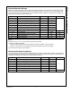
Electrical Characteristics
V
BIAS
(V
CC
, V
BS
)=15.0 V, T
A
= 25C, unless otherwise specified. The V
IN
and I
IN
parameters are referenced to COM.
The V
O
and I
O
parameters are referenced to V
S
and COM and are applicable to the respective outputs HO and LO.
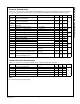
Dynamic Electrical Characteristics
V
BIAS
(V
CC
, V
BS
)=15.0 V, V
S
=COM, C
L
=1000pF and, T
A
= 25C, unless otherwise specified.
Note:
5. This parameter guaranteed by design.
Symbol Characteristics Test Condition Min. Typ. Max. Unit
V
CCUV+
V
BSUV+
V
CC
and V
BS
supply under-voltage
positive going threshold
8.2 9.2 10.0
V
V
CCUV-
V
BSUV-
V
CC
and V
BS
supply under-voltage
negative going threshold
7.6 8.7 9.6
V
CCUVH
V
BSUVH
V
CC
supply under-voltage lockout
hysteresis
0.6
I
LK
Offset supply leakage current V
B
=V
S
=200 V 50
µAI
QBS
Quiescent V
BS
supply current V
IN
=0V or 5 V 45 120
I
QCC
Quiescent V
CC
supply current V
IN
=0V or 5 V 70 180
I
PBS
Operating V
BS
supply current f
IN
=20 kHz, rms value 600
µA
I
PCC
Operating V
CC
supply current f
IN
=20 kHz, rms value 600
V
IH
Logic "1" input voltage 2.9
V
V
IL
Logic "0" input voltage 0.8
V
OH
High-level output voltage, V
BIAS
-V
O
I
O
=20 mA
1.0
V
OL
Low-level output voltage, V
O
0.6
I
IN+
Logic "1" input bias current V
IN
=5 V 10 20
µA
I
IN-
Logic "0" input bias current V
IN
=0 V 1.0 2.0
I
O+
Output high short-circuit pulsed current
V
O
=0 V, V
IN
=5 V with
PW<10 µs
250 350
mA
I
O-
Output low short-circuit pulsed current
V
O
=15 V, V
IN
=0 V with
PW<10 µs
500 650
V
S
Allowable negative V
S
pin voltage for
HIN signal propagation to HO
-9.8 -7.0 V
Symbol Characteristics Test Condition Min. Typ. Max. Unit
t
on
Turn-on propagation delay V
S
=0 V 100 170 300
ns
t
off
Turn-off propagation delay V
S
=0 V or 200 V
(5)
100 200 300
t
r
Turn-on rise time 20 60 140
t
f
Turn-off fall time 30 80
MT Delay matching, HS & LS turn-on/off 50