
Data Sheet

© 2006 Fairchild Semiconductor Corporation www.fairchildsemi.com
FAN7842 Rev. 1.5 3
FAN7842 High- and Low-Side Gate Driver
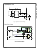
Pin Assignments
Figure 3. Pin Configuration (Top View)
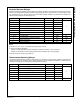
Pin Definitions
Name Description
V
CC
Low-Side Supply Voltage
HIN Logic Input for High-Side Gate Driver Output
LIN Logic Input for Low-Side Gate Driver Output
COM Logic Ground and Low-Side Driver Return
LO Low-Side Driver Output
V
S
High-Voltage Floating Supply Return
HO High-Side Driver Output
V
B
High-Side Floating Supply
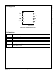
V
S
V
B
V
CC
LIN
HIN HO
LO
4
COM
3
2
1
5
6
7
8
FAN7842 Rev.01