
Data Sheet


© 2006 Fairchild Semiconductor Corporation www.fairchildsemi.com
FAN7842 Rev. 1.5 2
FAN7842 High- and Low-Side Gate Driver
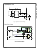
Typical Application Circuit
Figure 1. Application Circuit for Half-Bridge
Internal Block Diagram
Figure 2. Functional Block Diagram
D
BOOT
HIN
C
BOOT
15V
R
BOOT
Q1
R1
R2
V
B
HIN
COM
HO
V
S
LO
1
2
LIN
V
CC
5
6
8
3
4
7
R3
R4
600V
Q2
LIN
Load
FAN7842 Rev.01
C1
FAN7842 Rev.02
UVLO
DRIVER
PULSE
GENERATOR
3
1
4
8
6
V
CC
COM
LO
V
B
HO
V
S
R
R
S
Q
DRIVER
HS(ON/OFF)
LS(ON/OFF)
DELAY
UVLO
2
HIN
LIN
NOISE
CANCELLER
5
7
500K
500K