
Data Sheet


© 2009 Fairchild Semiconductor Corporation www.fairchildsemi.com
FAN7621 • Rev. 1.0.3 5
FAN7621 — PFM Controller for Half-Bridge Resonant Converters
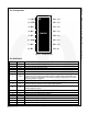
Electrical Characteristics
T
A
=25°C and LV
CC
=17V unless otherwise specified.
Symbol Parameter Test Conditions Min. Typ. Max. Unit
Supply Section
I
LK
Offset Supply Leakage Current HV
CC
=V
CTR
50 μA
I
Q
HV
CC
Quiescent HV
CC
Supply Current (HV
CC
UV+) - 0.1V 50 120 μA
I
Q
LV
CC
Quiescent LV
CC
Supply Current (LV
CC
UV+) - 0.1V 100 200 μA
I
O
HV
CC
Operating HV
CC
Supply Current
(RMS Value)
f
OSC
=100kHz, V
CON
> 0.6V,
C
Load
=1nF
5 8 mA
No Switching, V
CON
< 0.4V 100 200 μA
I
O
LV
CC
Operating LV
CC
Supply Current
(RMS Value)
f
OSC
=100kHz, V
CON
> 0.6V,
C
Load
=1nF
6 9 mA
No Switching, V
CON
< 0.4V 2 4 mA
UVLO Section
LV
CC
UV+ LV
CC
Supply Under-Voltage Positive Going Threshold (LV
CC
Start) 13.0 14.5 16.0 V
LV
CC
UV- LV
CC
Supply Under-Voltage Negative Going Threshold (LV
CC
Stop) 10.2 11.3 12.4 V
LV
CC
UVH LV
CC
Supply Under-Voltage Hysteresis 3.2 V
HV
CC
UV+ HV
CC
Supply Under-Voltage Positive Going Threshold (HV
CC
Start) 8.2 9.2 10.2 V
HV
CC
UV-
HV
CC
Supply Under-Voltage Negative Going Threshold (HV
CC
Stop)
7.8 8.7 9.6 V
HV
CC
UVH HV
CC
Supply Under-Voltage Hysteresis 0.5 V
Oscillator & Feedback Section
V
CONDIS
Control Pin Disable Threshold Voltage 0.36 0.40 0.44 V
V
CONEN
Control Pin Enable Threshold Voltage 0.54 0.60 0.66 V
V
RT
V-I Converter Threshold Voltage
R
T
=5.2kΩ
1.5 2.0 2.5 V
f
OSC
Output Oscillation Frequency 94 100 106 kHz
DC Output Duty Cycle 48 50 52 %
f
SS
Internal Soft-Start Initial Frequency
f
SS
=f
OSC
+40kHz, R
T
=5.2kΩ
140 kHz
t
SS
Internal Soft-Start Time 2 3 4 ms
Output Section
I
source
Peak Sourcing Current HV
CC
=17V 250 360 mA
I
sink
Peak Sinking Current HV
CC
=17V 460 600 mA
t
r
Rising Time
C
Load
=1nF, HV
CC
=17V
65 ns
t
f
Falling Time 35 ns
V
HOH
High Level of High-Side Gate Driving
Signal (V
HVCC
-V
HO
)
I
O
=20mA
1.0 V
V
HOL
Low Level of High-Side Gate Driving
Signal
0.6 V
V
LOH
High Level of High-Side Gate Driving
Signal (V
LVCC
-V
LO
)
1.0 V
V
LOL
Low Level of High-Side Gate Driving
Signal
0.6 V