
Data Sheet


© 2009 Fairchild Semiconductor Corporation www.fairchildsemi.com
FAN7621 • Rev. 1.0.3 3
FAN7621 — PFM Controller for Half-Bridge Resonant Converters
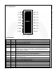
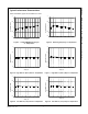
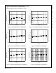
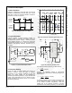
Pin Configuration
(3) HO
(4) NC
PG (16)
FAN7621
NC (13)
NC (15)
(5) NC
(6) CON
(7) NC
LO (14)
LV
CC
(12)
CS (9)
NC (11)
SG (10)
(2) CTR
(1) HV
CC
(8) R
T
Figure 3. Package Diagram
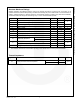
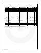
Pin Definitions
Pin # Name Description
1 HV
CC
This is the supply voltage of the high-side gate-drive circuit IC.
2 CTR This is the drain of the low-side MOSFET. Typically, a transformer is connected to this pin.
3 HO This is the high-side gate driving signal.
4 NC No connection.
5 NC No connection.
6 CON
This pin is for a protection and enabling/disabling the controller. When the voltage of this pin
is above 0.6V, the IC operation is enabled. When the voltage of this pin drops below 0.4V,
gate drive signals for both MOSFETs are disabled. When the voltage of this pin increases
above 5V, protection is triggered.
7 NC No connection.
8 R
T
This pin programs the switching frequency. Typically, an opto-coupler is connected to
control the switching frequency for the output voltage regulation.
9 CS
This pin senses the current flowing through the low-side MOSFET. Typically, negative
voltage is applied on this pin.
10 SG This pin is the control ground.
11 NC No connection.
12 LV
CC
This pin is the supply voltage of the control IC.
13 NC No connection.
14 LO This is the low-side gate driving signal.
15 NC No connection.
16 PG This pin is the power ground. This pin is connected to the source of the low-side MOSFET.