
Data Sheet

FAN7529 Critical Conduction Mode PFC Controller
© 2006 Fairchild Semiconductor Corporation www.fairchildsemi.com
FAN7529 Rev. 1.0.2 4
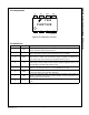
Absolute Maximum Ratings
Stresses exceeding the absolute maximum ratings may damage the device. The device may not function or be opera-
ble above the recommended operating conditions and stressing the parts to these levels is not recommended. In addi-
tion, extended exposure to stresses above the recommended operating conditions may affect device reliability. The
absolute maximum ratings are stress ratings only. T
A
= 25°C unless otherwise specified.
Thermal Impedance
(1)
Note:
1. Regarding the test environment and PCB type, please refer to JESD51-2 and JESD51-10.
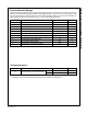
Symbol Parameter Value Unit
V
CC
Supply Voltage V
Z
V
I
OH
, I
OL
Peak Drive Output Current +500/-800 mA
I
clamp
Driver Output Clamping Diodes V
O
>V
CC
or V
O
<-0.3V ±10 mA
I
det
Detector Clamping Diodes ±10 mA
V
IN
Error Amplifier, MOT, CS Input Voltages -0.3 to 6 V
T
J
Operating Junction Temperature 150 °C
T
A
Operating Temperature Range -40 to 125 °C
T
STG
Storage Temperature Range -65 to 150 °C
V
ESD_HBM
ESD Capability, Human Body Model 2.0 kV
V
ESD_MM
ESD Capability, Machine Model 300 V
V
ESD_CDM
ESD Capability, Charged Device Model 500 V
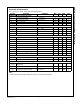
Symbol Parameter Value Unit
θ
JΑ
Thermal Resistance, Junction-to-Ambient
8-DIP 110 °C/W
8-SOP 150 °C/W