
Data Sheet

FAN7529 Critical Conduction Mode PFC Controller
© 2006 Fairchild Semiconductor Corporation www.fairchildsemi.com
FAN7529 Rev. 1.0.2 3
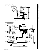
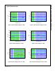
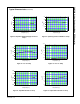
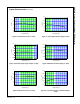
Pin Assignments
Figure 3. Pin Configuration (Top View)
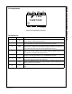
Pin Definitions
Pin # Name Description
1INV
This pin is the inverting input of the error amplifier. The output voltage of the boost PFC
converter should be resistively divided to 2.5V.
2COMP
This pin is the output of the transconductance error amplifier. Components for output
voltage compensation should be connected between this pin and GND.
3MOT
This pin is used to set the slope of the internal ramp. The voltage of this pin is main-
tained at 2.9V. If a resistor is connected between this pin and GND, current flows out of
the pin and the slope of the internal ramp is proportional to this current.
4CS
This pin is the input of the over-current protection comparator. The MOSFET current is
sensed using a sensing resistor and the resulting voltage is applied to this pin. An
internal RC filter is included to filter switching noise.
5ZCD
This pin is the input of the zero current detection block. If the voltage of this pin goes
higher than 1.5V, then goes lower than 1.4V, the MOSFET is turned on.
6GND
This pin is used for the ground potential of all the pins. For proper operation, the signal
ground and the power ground should be separated.
7OUT
This pin is the gate drive output. The peak sourcing and sinking current levels are
+500mA and -800mA respectively. For proper operation, the stray inductance in the
gate driving path must be minimized.
8V
CC
This pin is the IC supply pin. IC current and MOSFET drive current are supplied using
this pin.
FAN7529
6 58 7
V
CC
OUT GND ZCD
1 2 3 4
COMP CSMOTINV
YWW
FAN7529 Rev. 00