
Data Sheet

© 2009 Fairchild Semiconductor Corporation www.fairchildsemi.com
FAN5400 Family • Rev. 1.10 7
FAN5400 Family — USB-Compliant Single-Cell Li-Ion Switching Charger with USB-OTG Boost Regulator
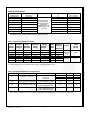
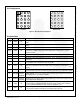
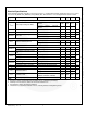
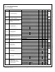
Electrical Specifications
Unless otherwise specified: according to the circuit of Figure 1; recommended operating temperature range for T
J
and T
A
;
V
BUS
=5.0 V; HZ_MODE; OPA_MODE=0; (Charge Mode); SCL, SDA, OTG=0 or 1.8 V; and typical values are for T
J
=25°C.
Symbol
Parameter
Conditions
Min.
Typ.
Max.
Units
Input Power Source Detection
V
IN(MIN)1
VBUS Input Voltage Rising
To Initiate and Pass VBUS Validation
4.29
4.42
V
V
IN(MIN)2
Minimum VBUS during Charge
During Charging
3.71
3.94
V
t
VBUS_VALID
VBUS Validation Time
30
ms
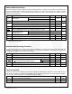
Special Charger (V
BUS
) (FAN5403 – FAN5405)
V
SP
Special Charger Setpoint Accuracy
–3
+3
%
Input Current Limit
I
INLIM
Input Current Limit Threshold
I
IN
Set to 100 mA
88
93
98
mA
I
IN
Set to 500 mA
450
475
500
V
REF
Bias Generator
V
REF
Bias Regulator Voltage
V
BUS
> V
IN(MIN)
or V
BAT
> V
BAT(MIN)
6.5
V
Short-Circuit Current Limit
20
mA
Battery Recharge Threshold
V
RCH
Recharge Threshold
Below V
(OREG)
100
120
150
mV
Deglitch Time
V
BAT
Falling Below V
RCH
Threshold
130
ms
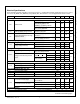
STAT Output
V
STAT(OL)
STAT Output Low
I
STAT
=10 mA
0.4
V
I
STAT(OH)
STAT High Leakage Current
V
STAT
=5 V
1
A
Battery Detection
I
DETECT
Battery Detection Current before
Charge Done (Sink Current)
(5)
Begins after Termination Detected
and V
BAT
< V
OREG
–V
RCH
–0.80
mA
t
DETECT
Battery Detection Time
262
ms
Sleep Comparator
V
SLP
Sleep-Mode Entry Threshold,
V
BUS
– V
BAT
2.3 V < V
BAT
< V
OREG
, V
BUS
Falling
0
0.04
0.10
V
V
SLP_EXIT
Deglitch Time for VBUS Rising
Above V
SLP
+ V
SLP_EXIT
Rising Voltage
30
ms
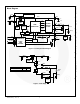
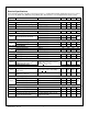
Power Switches (see Figure 3)
R
DS(ON)
Q3 On Resistance (VBUS to PMID)
I
IN(LIMIT)
=500 mA
180
250
mΩ
Q1 On Resistance (PMID to SW)
130
225
Q2 On Resistance (SW to GND)
150
225
Charger PWM Modulator
f
SW
Oscillator Frequency
2.7
3.0
3.3
MHz
D
MAX
Maximum Duty Cycle
100
%
D
MIN
Minimum Duty Cycle
0
%
I
SYNC
Synchronous to Non-Synchronous
Current Cut-Off Threshold
(6)
Low-Side MOSFET (Q2) Cycle-by-
Cycle Current Limit
140
mA
Continued on the following page…