
Data Sheet

© 2009 Fairchild Semiconductor Corporation www.fairchildsemi.com
FAN5400 Family • Rev. 1.10 5
FAN5400 Family — USB-Compliant Single-Cell Li-Ion Switching Charger with USB-OTG Boost Regulator
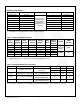
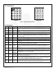
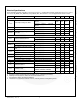
Absolute Maximum Ratings
Stresses exceeding the absolute maximum ratings may damage the device. The device may not function or be operable above
the recommended operating conditions and stressing the parts to these levels is not recommended. In addition, extended
exposure to stresses above the recommended operating conditions may affect device reliability. The absolute maximum
ratings are stress ratings only.
Symbol
Parameter
Min.
Max.
Unit
V
BUS
VBUS Voltage
Continuous
–1.4
20.0
V
Pulsed, 100 ms Maximum Non-Repetitive
–2.0
V
STAT
STAT Voltage
–0.3
16.0
V
V
I
PMID Voltage
7.0
V
SW, CSIN, VBAT, AUXPWR, DISABLE Voltage
–0.3
7.0
V
O
Voltage on Other Pins
–0.3
6.5
(4)
V
dt
dV
BUS
Maximum VBUS Slope above 5.5 V when Boost or Charger are Active
4
V/s
ESD
Electrostatic Discharge
Protection Level
Human Body Model per JESD22-A114
2000
V
Charged Device Model per JESD22-C101
500
T
J
Junction Temperature
–40
+150
°C
T
STG
Storage Temperature
–65
+150
°C
T
L
Lead Soldering Temperature, 10 Seconds
+260
°C
Note:
4. Lesser of 6.5 V or V
I
+ 0.3 V.
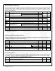
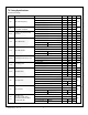
Recommended Operating Conditions
The Recommended Operating Conditions table defines the conditions for actual device operation. Recommended operating
conditions are specified to ensure optimal performance to the datasheet specifications. Fairchild does not recommend
exceeding them or designing to absolute maximum ratings.
Symbol
Parameter
Min.
Max.
Units
V
BUS
Supply Voltage
4
6
V
V
BAT(MAX)
Maximum Battery Voltage when Boost enabled
4.5
V
dt
dV
BUS
Negative VBUS Slew Rate during VBUS Short Circuit,
C
MID
< 4.7 F, see VBUS Short While Charging
T
A
< 60°C
4
V/s
T
A
> 60°C
2
T
A
Ambient Temperature
–30
+85
°C
T
J
Junction Temperature (see Thermal Regulation and Protection section)
–30
+120
°C
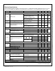
Thermal Properties
Junction-to-ambient thermal resistance is a function of application and board layout. This data is measured with four-layer
2s2p boards in accordance to JEDEC standard JESD51. Special attention must be paid not to exceed junction temperature
T
J(max)
at a given ambient temperature T
A
. For measured data, see Table 11.
Symbol
Parameter
Typical
Units
JA
Junction-to-Ambient Thermal Resistance
60
°C/W
JB
Junction-to-PCB Thermal Resistance
20
°C/W