
Data Sheet

© 2009 Fairchild Semiconductor Corporation www.fairchildsemi.com
FAN5400 Family • Rev. 1.10 4
FAN5400 Family — USB-Compliant Single-Cell Li-Ion Switching Charger with USB-OTG Boost Regulator
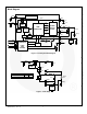
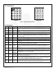
Pin Configuration
C1
B1
A1 A2
C3
B3
A3
C2
D1 D3D2
B2
C4
B4
A4
D4
E1 E3E2 E4
Top View
C1
B1
A1
C3
B3
A3 A2
C2
D1D3 D2
B2
C4
B4
A4
D4
E1E3 E2E4
Bottom View
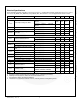
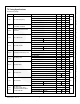
Figure 4. WLCSP-20 Pin Assignments
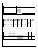
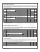
Pin Definitions
Pin #
Name
Part #
Description
A1, A2
VBUS
ALL
Charger Input Voltage and USB-OTG output voltage. Bypass with a 1 F capacitor to
PGND.
A3
NC
ALL
No Connect. No external connection is made between this pin and the IC’s internal
circuitry.
A4
SCL
ALL
I
2
C Interface Serial Clock. This pin should not be left floating.
B1-B3
PMID
ALL
Power Input Voltage. Power input to the charger regulator, bypass point for the input
current sense, and high-voltage input switch. Bypass with a minimum of 4.7 F, 6.3 V
capacitor to PGND.
B4
SDA
ALL
I
2
C Interface Serial Data. This pin should not be left floating.
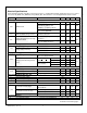
C1-C3
SW
ALL
Switching Node. Connect to output inductor.
C4
STAT
ALL
Status. Open-drain output indicating charge status. The IC pulls this pin LOW when charge
is in process.
D1-D3
PGND
ALL
Power Ground. Power return for gate drive and power transistors. The connection from this
pin to the bottom of C
MID
should be as short as possible.
D4
OTG
ALL
On-The-Go. Enables boost regulator in conjunction with OTG_EN and OTG_PL bits (see
Table 16). On VBUS Power-On Reset (POR), this pin sets the input current limit for t
15MIN
charging.
E1
CSIN
ALL
Current-Sense Input. Connect to the sense resistor in series with the battery. The IC uses
this node to sense current into the battery. Bypass this pin with a 0.1 F capacitor to PGND.
E2
AUXPWR
FAN5400,
FAN5401,
FAN5402
Auxiliary Power. Connect to the battery pack to provide IC power during High-Impedance
Mode. Bypass with a 1 F capacitor to PGND.
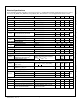
E2
DISABLE
FAN5403,
FAN5404,
FAN5405
Charge Disable. If this pin is HIGH, charging is disabled. When LOW, charging is
controlled by the I
2
C registers. When this pin is HIGH, the 15-minute timer is reset. This pin
does not affect the 32-second timer.
E3
VREG
ALL
Regulator Output. Connect to a 1F capacitor to PGND. This pin can supply up to 2 mA of
DC load current. For FAN5400-FAN5402, the output voltage is PMID, which is limited to
6.5 V. For FAN5403-FAN5405, the output voltage is regulated to 1.8 V.
E4
VBAT
ALL
Battery Voltage. Connect to the positive (+) terminal of the battery pack. Bypass with a
0.1 F capacitor to PGND if the battery is connected through long leads.