
Data Sheet

© 2009 Fairchild Semiconductor Corporation www.fairchildsemi.com
FAN5400 Family • Rev. 1.10 34
FAN5400 Family — USB-Compliant Single-Cell Li-Ion Switching Charger with USB-OTG Boost Regulator
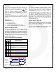
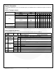
Table 23. Register Bit Definitions (Continued)
SP_CHARGER (FAN5403 – FAN5405)
Register Address: 05
Default Value=001X X100
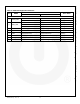
7
Reserved
0
R
Unused
6
DIS_VREG
0
R/W
1.8 V regulator is ON
1
1.8 V regulator is OFF
5
IO_LEVEL
0
R/W
Output current is controlled by IOCHARGE bits
1
Voltage across R
SENSE
for output current control is set to 22.1 mV (325 mA for
R
SENSE
=68 m, 221 mA for 100 m)
4
SP
0
R
Special charger is not active (V
BUS
is able to stay above V
SP
)
1
Special charger has been detected and V
BUS
is being regulated to V
SP
3
EN_LEVEL
0
R
DISABLE pin is LOW
1
DISABLE pin is HIGH
2:0
VSP
Table 8
R/W
Special charger input regulation voltage, see Table 8
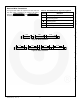
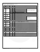
SAFETY (FAN5403 – FAN5405)
Register Address: 06
Default Value=0100 0000 (40h)
7
Reserved
0
R
Bit disabled and always returns 0 when read back
6:4
ISAFE
Table 9
R/W
Sets the maximum I
OCHARGE
value used by the control circuit, see Table 9
3:0
VSAFE
Table 10
R/W
Sets the maximum V
OREG
used by the control circuit, see Table 10
MONITOR
Register Address: 10h (16)
See Table 19
7
ITERM_CMP
See
Table 19
R
Real-time ITERM comparator output: 1 when VRSENSE > ITERM reference.
Dynamic system loads can cause this bit to toggle between 0 and 1.
6
VBAT_CMP
R
Output of VBAT comparator
5
LINCHG
R
30 mA linear charger ON
4
T_120
R
Thermal regulation comparator; when=1 and T_145=0, the charge current is limited
to 22.1 mV across R
SENSE
3
ICHG
R
0 indicates the I
CHARGE
loop is controlling the battery charge current
2
IBUS
R
0 indicates the I
BUS
(input current) loop is controlling the battery charge current
1
VBUS_VALID
R
1 indicates V
BUS
has passed validation and is capable of charging
0
CV
R
1 indicates the constant-voltage loop (OREG) is controlling the charger and all
current limiting loops have released