
Data Sheet

© 2009 Fairchild Semiconductor Corporation www.fairchildsemi.com
FAN5400 Family • Rev. 1.10 33
FAN5400 Family — USB-Compliant Single-Cell Li-Ion Switching Charger with USB-OTG Boost Regulator
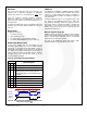
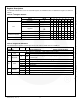
Table 23. Register Bit Definitions (Continued)
Bit
Name
Value
Type
Description
CONTROL1
Register Address: 01
Default Value=0011 0000 (30h)
7:6
I
INLIM
R/W
Input current limit, see Table 7
5:4
V
LOWV
00
R/W
3.4 V
Weak battery voltage threshold
01
3.5 V
10
3.6 V
11
3.7 V
3
TE
0
R/W
Disable charge current termination
1
Enable charge current termination
2
CE
0
R/W
Charger enabled
1
Charger disabled
1
HZ_MODE
0
R/W
Not High-Impedance Mode
See Table 16
1
High-Impedance Mode
0
OPA_MODE
0
R/W
Charge Mode
1
Boost Mode
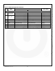
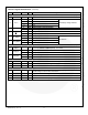
OREG
Register Address: 02
Default Value=0000 1010 (0Ah)
7:2
OREG
R/W
Charger output “float” voltage; programmable from 3.5 to 4.44 V in 20 mV
increments; defaults to 000010 (3.54 V), see Table 3
1
OTG_PL
0
R/W
OTG pin active LOW
1
OTG pin active HIGH
0
OTG_EN
0
R/W
Disables OTG pin
1
Enables OTG pin
IC_INFO
Register Address: 03 or 3B
Default Value=100X XXXX
7:5
Vendor Code
100
R
Identifies Fairchild Semiconductor as the IC supplier
4:3
PN
R
Part number bits, see the Ordering Info on page 1
2:0
REV
R
IC Revision, revision 1.X, where X is the decimal of these three bits
IBAT
Register Address: 04
Default Value=1000 1001 (89h)
7
RESET
1
W
Writing a 1 resets charge parameters, except the Safety register (Reg6), to their
defaults: writing a 0 has no effect; read returns 1
6:4
IOCHARGE
Table 5
R/W
Programs the maximum charge current, see Table 5
3
Reserved
1
R
Unused
2:0
ITERM
Table 6
R/W
Sets the current used for charging termination, see Table 6