
Data Sheet

© 2009 Fairchild Semiconductor Corporation www.fairchildsemi.com
FAN5400 Family • Rev. 1.10 32
FAN5400 Family — USB-Compliant Single-Cell Li-Ion Switching Charger with USB-OTG Boost Regulator
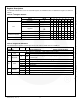
Register Descriptions
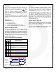
The FAN5400-FAN5402 have seven user-accessible registers; the FAN5403-05 have an additional two registers, as defined in
Table 22.
Table 22. I
2
C Register Address
IC
Register
Address Bits
Name
REG#
7
6
5
4
3
2
1
0
ALL
CONTROL0
0
0
0
0
0
0
0
0
0
CONTROL1
1
0
0
0
0
0
0
0
1
OREG
2
0
0
0
0
0
0
1
0
IC_INFO
03
or
3Bh
0
0
0
0
0
0
1
1
IBAT
4
0
0
0
0
0
1
0
0
FAN5403-FAN5405
SP_CHARGER
5
0
0
0
0
0
1
0
1
SAFETY
6
0
0
0
0
0
1
1
0
ALL
MONITOR
10h
0
0
0
0
1
0
1
0
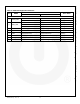
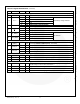
Table 23. Register Bit Definitions
This table defines the operation of each register bit for all IC versions. Default values are in bold text.
Bit
Name
Value
Type
Description
CONTROL0
Register Address: 00
Default Value=X1XX 0XXX
7
TMR_RST
OTG
1
W
Writing a 1 resets the t
32S
timer; writing a 0 has no effect
R
Returns the OTG pin level (1=HIGH)
6
EN_STAT
0
R/W
Prevents STAT pin from going LOW during charging; STAT pin still pulses to
enunciate faults
1
Enables STAT pin LOW when IC is charging
5:4
STAT
00
R
Ready
01
Charge in progress
10
Charge done
11
Fault
3
BOOST
0
R
IC is not in Boost Mode
1
IC is in Boost Mode
2:0
FAULT
R
Fault status bits: for Charge Mode, see Table 13; for Boost Mode: see Table 18