
Data Sheet

© 2009 Fairchild Semiconductor Corporation www.fairchildsemi.com
FAN5400 Family • Rev. 1.10 31
FAN5400 Family — USB-Compliant Single-Cell Li-Ion Switching Charger with USB-OTG Boost Regulator
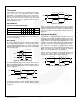
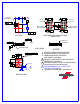
Read and Write Transactions
The figures below outline the sequences for data read and
write. Bus control is signified by the shading of the packet,
defined as
Master Drives Bus
and
Slave Drives Bus
.
All addresses and data are MSB first.
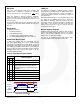
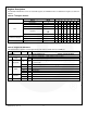
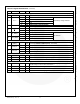
Table 21. Bit Definitions for Figure 49, Figure 50
Symbol
Definition
S
START, see Figure 46.
A
ACK. The slave drives SDA to 0 to acknowledge
the preceding packet.
A
NACK. The slave sends a 1 to NACK the
preceding packet.
R
Repeated START, see Figure 48
P
STOP, see Figure 47
S Slave Address A Reg Addr A A P0
7 bits 8 bits 8 bits
Data
0 0 0
Figure 49. Write Transaction
S Slave Address A Reg Addr A0
7 bits 8 bits
R Slave Address
7 bits
1 A Data A
8 bits
0 0 0 1
P
Figure 50. Read Transaction