
Data Sheet

© 2009 Fairchild Semiconductor Corporation www.fairchildsemi.com
FAN5400 Family • Rev. 1.10 28
FAN5400 Family — USB-Compliant Single-Cell Li-Ion Switching Charger with USB-OTG Boost Regulator
BST State
This is the normal operating mode of the regulator. The
regulator uses a minimum t
OFF
-minimum t
ON
modulation
scheme. The minimum t
OFF
is proportional to
OUT
IN
V
V
, which
keeps the regulator’s switching frequency reasonably
constant in CCM. t
ON(MIN)
is proportional to V
BAT
and is a
higher value if the inductor current reached 0 before t
OFF(MIN)
in the prior cycle.
To ensure the VBUS does not pump significantly above the
regulation point, the boost switch remains off as long as
FB > V
REF
.
Boost Faults
If a BOOST fault occurs:
1. The STAT pin pulses.
2. OPA_MODE bit is reset.
3. The power stage is in High-Impedance Mode.
4. The FAULT bits (REG0[2:0]) are set per Table 18.
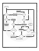
Restart After Boost Faults
If boost was enabled with the OPA_MODE bit and
OTG_EN=0, Boost Mode can only be enabled through
subsequent I
2
C commands since OPA_MODE is reset on
boost faults. If OTG_EN=1 and the OTG pin is still ACTIVE
(see Table 16), the boost restarts after a 5.2 ms delay, as
shown in Figure 44. If the fault condition persists, restart is
attempted every 5 ms until the fault clears or an I
2
C
command disables the boost.
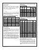
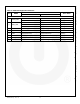
Table 18. Fault Bits During Boost Mode
Fault Bit
Fault Description
B2
B1
B0
0
0
0
Normal (no fault)
0
0
1
V
BUS
> VBUS
OVP
0
1
0
V
BUS
fails to achieve the voltage required to
advance to the next state during soft-start
or sustained (>50 s) current limit during the
BST state.
0
1
1
V
BAT
< UVLO
BST
1
0
0
N/A: This code does not appear.
1
0
1
Thermal shutdown
1
1
0
Timer fault; all registers reset.
1
1
1
N/A: This code does not appear.
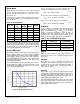
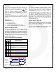
450mA
VBUS
BATTERY
CURRENT
0
560
BOOST
ENABLED
0
64
5200
Figure 44. Boost Response Attempting to Start into V
BUS
Short Circuit (Times in s)
VREG Pin
The VREG pin on FAN5400 - FAN5402 provides a voltage
protected from over-voltage surges on VBUS, which can be
used to run auxiliary circuits. This voltage is essentially a
current-limited replica of PMID. The maximum voltage on
this node is 5.9 V.
FAN5403-FAN5405 provide a 1.8 V regulated output on this
pin, which can be disabled through I
2
C by setting the
DIS_VREG bit (REG5[6]). VREG can supply up to 2 mA.
This circuit, which is powered from PMID, is enabled only
when PMID > V
BAT
and does not drain current from the
battery. During boost, V
REG
is off. It is also off when the
HZ_MODE bit (REG1[1])=1.
Monitor Register (Reg10h)
Additional status monitoring bits enable the host processor
to have more visibility into the status of the IC. The monitor
bits are real-time status indicators and are not internally
debounced or otherwise time qualified.
The state of the MONITOR register bits listed in High-
Impedance Mode are only valid when V
BUS
is valid.