
Data Sheet

© 2009 Fairchild Semiconductor Corporation www.fairchildsemi.com
FAN5400 Family • Rev. 1.10 27
FAN5400 Family — USB-Compliant Single-Cell Li-Ion Switching Charger with USB-OTG Boost Regulator
Boost Mode
Boost Mode can be enabled if the IC is in 32-Second Mode
with the OTG pin and OPA_MODE bits as indicated in Table
16. The OTG pin ACTIVE state is 1 if OTG_PL=1 and 0
when OTG_PL=0.
If boost is active using the OTG pin, Boost Mode is initiated
even if the HZ_MODE=1. The HZ_MODE bit overrides the
OPA_MODE bit.
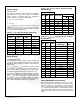
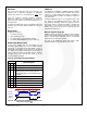
Table 16. Enabling Boost
OTG_EN
OTG
Pin
HZ_
MODE
OPA_
MODE
BOOST
1
ACTIVE
X
X
Enabled
X
X
0
1
Enabled
X
ACTIVE
X
0
Disabled
0
X
1
X
Disabled
1
ACTIVE
1
1
Disabled
0
ACTIVE
0
0
Disabled
To remain in Boost Mode, the TMR_RST must be set by the
host before the t
32S
timer times out. If t
32S
times out in Boost
Mode; the IC resets all registers, pulses the STAT pin, sets
the FAULT bits to 110, and resets the BOOST bit. VBUS
POR or reading R0 clears the fault condition.
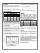
Boost PWM Control
The IC uses a minimum on-time and computed minimum off-
time to regulate VBUS. The regulator achieves excellent
transient response by employing current-mode modulation.
This technique causes the regulator to exhibit a load line.
During PWM Mode, the output voltage drops slightly as the
input current rises. With a constant V
BAT
, this appears as a
constant output resistance.
The “droop” caused by the output resistance when a load is
applied allows the regulator to respond smoothly to load
transients with no undershoot from the load line. This can be
seen in Figure 33 and Figure 43.
200
225
250
275
300
325
350
2.0 2.5 3.0 3.5 4.0 4.5 5.0
Battery Voltage, VBAT (V)
Output Resistance (m
W
)
Figure 43. Output Resistance (R
OUT
)
V
BUS
as a function of I
LOAD
can be computed when the
regulator is in PWM Mode (continuous conduction) as:
LOADOUTOUT
IR07.5V
EQ. 1
At V
BAT
=3.3 V, and I
LOAD
=200 mA, V
BUS
would drop to:
V018.52.026.007.5V
OUT
EQ. 1A
At V
BAT
=2.7V, and I
LOAD
=200mA, V
BUS
would drop to:
V005.52.0327.007.5V
OUT
EQ. 1B
PFM Mode
If V
BUS
> VREF
BOOST
(nominally 5.07 V) when the minimum
off-time has ended, the regulator enters PFM Mode. Boost
pulses are inhibited until V
BUS
< VREF
BOOST
. The minimum
on-time is increased to enable the output to pump up
sufficiently with each PFM boost pulse. Therefore the
regulator behaves like a constant on-time regulator, with the
bottom of its output voltage ripple at 5.07 V in PFM Mode.
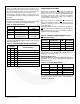
Table 17. Boost PWM Operating States
Mode
Description
Invoked When
LIN
Linear Startup
V
BAT
> V
BUS
SS
Boost Soft-Start
V
BUS
< V
BST
BST
Boost Operating Mode
V
BAT
> UVLO
BST
and
SS Completed
Startup
When the boost regulator is shut down, current flow is
prevented from V
BAT
to V
BUS
, as well as reverse flow from
V
BUS
to V
BAT
.
LIN State
When EN rises, if V
BAT
> UVLO
BST
, the regulator first
attempts to bring PMID within 400 mV of V
BAT
using an
internal 450 mA current source from VBAT (LIN State). If
PMID has not achieved V
BAT
– 400 mV after 560 s, a
FAULT state is initiated.
SS State
When PMID > V
BAT
– 400 mV, the boost regulator begins
switching with a reduced peak current limit of about 50% of
its normal current limit. The output slews up until V
BUS
is
within 5% of its set point; at which time, the regulation loop is
closed and the current limit is set to 100%.
If the output fails to achieve 95% of its set point (V
BST
) within
128 s, the current limit is increased to 100%. If the output
fails to achieve 95% of its set point after this second 384 s
period, a fault state is initiated.