
Data Sheet

© 2009 Fairchild Semiconductor Corporation www.fairchildsemi.com
FAN5400 Family • Rev. 1.10 24
FAN5400 Family — USB-Compliant Single-Cell Li-Ion Switching Charger with USB-OTG Boost Regulator
Special Charger
FAN5403-05 Only
The FAN5403, FAN5404, and FAN5405 have additional
functionality to limit input current in case a current-limited
“special charger” is supplying VBUS. The FAN5403-05
slowly increases the charging current until either:
I
INLIM
or I
OCHARGE
is reached
or
V
BUS
=V
SP
.
If V
BUS
collapses to V
SP
when the current is ramping up, the
FAN5403-05 charge with an input current that keeps
V
BUS
=V
SP
. When the V
SP
control loop is limiting the charge
current, the SP bit (REG5[4]) is set.
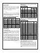
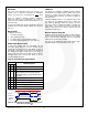
Table 8. V
SP
as Function of SP Bits (REG5[2:0])
SP (REG5[2:0])
DEC
BIN
HEX
V
SP
0
000
00
4.213
1
001
01
4.293
2
010
02
4.373
3
011
03
4.453
4
100
04
4.533
5
101
05
4.613
6
110
06
4.693
7
111
07
4.773
Safety Settings
FAN5403-FAN5405 Only
The FAN5403-05 contain a SAFETY register (REG6) that
prevents the values in OREG (REG2[7:2]) and IOCHARGE
(REG4[6:4]) from exceeding the values of the VSAFE and
ISAFE values.
After V
BAT
exceeds V
SHORT
, the SAFETY register is loaded
with its default value and may be written only before any
other register is written. After writing to any other register,
the SAFETY register is locked until V
BAT
falls below V
SHORT
.
The ISAFE (REG6[6:4]) and VSAFE (REG6[3:0]) registers
establish values that limit the maximum values of I
OCHARGE
and V
OREG
used by the control logic. If the host attempts to
write a value higher than VSAFE or ISAFE to OREG or
IOCHARGE, respectively; the VSAFE, ISAFE value appears
as the OREG, IOCHARGE register value, respectively.
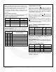
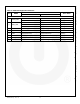
Table 9. I
SAFE
(I
OCHARGE
Limit) as Function of ISAFE
Bits (REG6[6:4])
ISAFE (REG6[6:4])
DEC
BIN
HEX
V
RSENSE
(mV)
I
SAFE
(mA)
68 m
100 m
0
000
00
37.4
550
374
1
001
01
44.2
650
442
2
010
02
51.0
750
510
3
011
03
57.8
850
578
4
100
04
64.6
950
646
5
101
05
71.4
1050
714
6
110
06
78.2
1150
782
7
111
07
85.0
1250
850
Table 10. V
SAFE
(V
OREG
Limit) as Function of VSAFE
Bits (REG6[3:0])
VSAFE (REG6[3:0])
DEC
BIN
HEX
Max. OREG
(REG2[7:2])
VOREG
Max.
0
0000
00
100011
4.20
1
0001
01
100100
4.22
2
0010
02
100101
4.24
3
0011
03
100110
4.26
4
0100
04
100111
4.28
5
0101
05
101000
4.30
6
0110
06
101001
4.32
7
0111
07
101010
4.34
8
1000
08
101011
4.36
9
1001
09
101100
4.38
10
1010
0A
101101
4.40
11
1011
0B
101110
4.42
12
1100
0C
101111
4.44
13
1101
0D
110000
4.44
14
1110
0E
110001
4.44
15
1111
0F
110010
4.44
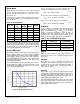
Thermal Regulation and Protection
When the IC’s junction temperature reaches T
CF
(about
120°C), the charger reduces its output current to 550 mA to
prevent overheating. If the temperature increases beyond
T
SHUTDOWN
; charging is suspended, the FAULT bits are set to
101, and STAT is pulsed HIGH. In Suspend Mode, all timers
stop and the state of the IC’s logic is preserved. Charging
resumes at programmed current after the die cools to about
120°C.