
Data Sheet

© 2009 Fairchild Semiconductor Corporation www.fairchildsemi.com
FAN5400 Family • Rev. 1.10 19
FAN5400 Family — USB-Compliant Single-Cell Li-Ion Switching Charger with USB-OTG Boost Regulator
PWM Controller in Charge Mode
The IC uses a current-mode PWM controller to regulate the
output voltage and battery charge currents. The synchronous
rectifier (Q2) has a negative current limit that turns off Q2 at
140 mA to prevent current flow from the battery.
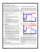
Safety Timer
This section references Figure 41 and Figure 42.
At the beginning of charging, the IC starts a 15-minute timer
(t
15MIN
). When this timer times out, charging is terminated.
Writing to any register through I
2
C stops and resets the t
15MIN
timer, which in turn starts a 32-second timer (t
32S
). Setting
the TMR_RST bit (REG0[7]) resets the t
32S
timer. If the t
32S
timer times out, charging is terminated, the registers are set
to their default values, and charging resumes using the
default values with the t
15MIN
timer running.
Normal charging is controlled by the host with the t
32S
timer
running to ensure that the host is alive. Charging with the
t
15MIN
timer running is used for charging that is unattended by
the host. If the t
15MIN
timer expires, the IC turns off the
charger, sets the
CE
bit, and indicates a timer fault (110) on
the FAULT bits (REG0[2:0]). This sequence prevents
overcharge if the host fails to reset the t
32S
timer.
V
BUS
POR / Non-Compliant Charger Rejection
When the IC detects that V
BUS
has risen above V
IN(MIN)1
(4.4 V), the IC applies a 110 load from VBUS to GND. To
clear the VBUS POR (Power-On-Reset) and begin charging,
VBUS must remain above V
IN(MIN)1
and below VBUS
OVP
for
t
VBUS_VALID
(30 ms) before the IC initiates charging. The
VBUS validation sequence always occurs before charging is
initiated or re-initiated (for example, after a VBUS OVP fault
or a V
RCH
recharge initiation).
t
VBUS_VALID
ensures that unfiltered 50 / 60 Hz chargers and
other non-compliant chargers are rejected.
USB-Friendly Boot Sequence
For all versions except FAN5401, FAN5404
At VBUS POR, when the battery voltage is above the weak
battery threshold (V
LOWV
), the IC operates in accordance with
its I
2
C register settings. If V
BAT
< V
LOWV
, the IC sets all
registers to their default values and enables the charger
using an input current limit controlled by the OTG pin
(100 mA if OTG is LOW and 500 mA if OTG is HIGH). This
feature can revive a battery whose voltage is too low to
ensure reliable host operation. Charging continues in the
absence of host communication even after the battery has
reached V
OREG
, whose default value is 3.54 V, and the
charger remains active until t
15MIN
times out. Once the host
processor begins writing to the IC, charging parameters are
set by the host, which must continually reset the t
32S
timer to
continue charging using the programmed charging
parameters. If t
32S
.times out, the register defaults are loaded,
the FAULT bits are set to 110, STAT is pulsed HIGH, and
charging continues with default charge parameters.
The FAN5401 and FAN5404 do not automatically initiate
charging at VBUS POR. Instead, they wait for the host to
initiate charging through I
2
C commands.
Input Current Limiting
To minimize charging time without overloading VBUS current
limitations, the IC’s input current limit can be programmed by
the I
INLIM
bits (REG1[7:6]).
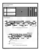
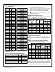
Table 7. Input Current Limit
I
INLIM
REG1[7:6]
Input Current Limit
00
100 mA
01
500 mA
10
800 mA
11
No limit
For all versions except the FAN5401 and FAN5404, the OTG
pin establishes the input current limit when t
15MIN
is running.
For the FAN5401 and FAN5404, no charging occurs
automatically at VBUS POR, so the input current limit is
established by the I
INLIM
bits.