
Data Sheet

© 2009 Fairchild Semiconductor Corporation www.fairchildsemi.com
FAN5400 Family • Rev. 1.10 10
FAN5400 Family — USB-Compliant Single-Cell Li-Ion Switching Charger with USB-OTG Boost Regulator
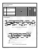
I
2
C Timing Specifications
Guaranteed by design.
Symbol
Parameter
Conditions
Min.
Typ.
Max.
Units
t
FDA
SDA Fall Time
Standard Mode
20 + 0.1C
B
300
ns
Fast Mode
20 + 0.1C
B
300
High-Speed Mode, C
B
< 100 pF
10
80
High-Speed Mode, C
B
< 400 pF
20
160
t
SU;STO
Stop Condition Setup Time
Standard Mode
4
s
Fast Mode
600
ns
High-Speed Mode
160
ns
C
B
Capacitive Load for SDA, SCL
400
pF
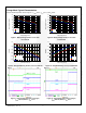
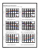
Timing Diagrams
START
REPEATED
START
SCL
SDA
t
F
t
HD;STA
t
LOW
t
R
t
HD;DAT
t
HIGH
T
SU;DAT
t
SU;STA
t
HD;STO
t
BUF
START STOP
t
HD;STA
Figure 5. I
2
C Interface Timing for Fast and Slow Modes
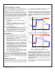
REPEATED
START
SCLH
SDAH
t
FDA
t
LOW
t
RCL1
t
HD;DAT
t
HIGH
t
SU;STO
REPEATED
START
t
RDA
t
FCL
t
SU;DAT
t
RCL
STOP
= MCS Current Source Pull-up
= R
P
Resistor Pull-up
note A
Note A: First rising edge of SCLH after Repeated Start and after each ACK bit.
t
HD;STA
t
SU;STA
Figure 6. I
2
C Interface Timing for High-Speed Mode