Is Now Part of To learn more about ON Semiconductor, please visit our website at www.onsemi.com Please note: As part of the Fairchild Semiconductor integration, some of the Fairchild orderable part numbers will need to change in order to meet ON Semiconductor’s system requirements. Since the ON Semiconductor product management systems do not have the ability to manage part nomenclature that utilizes an underscore (_), the underscore (_) in the Fairchild part numbers will be changed to a dash (-).
FAN5400 / FAN5401 / FAN5402 / FAN5403 / FAN5404 / FAN5405 USB-Compliant Single-Cell Li-Ion Switching Charger with USB-OTG Boost Regulator Features Description Fully Integrated, High-Efficiency Charger for Single-Cell Li-Ion and Li-Polymer Battery Packs Faster Charging than Linear The FAN5400 family (FAN540x) combines a highly integrated switch-mode charger, to minimize single-cell Lithium-ion (Li-ion) charging time from a USB power source, and a boost regulator to power a USB peripheral from the
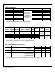
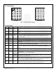
Part Number Temperature Range FAN5400UCX -40 to 85°C FAN5401UCX -40 to 85°C FAN5402UCX -40 to 85°C FAN5403UCX -40 to 85°C (1) Package PN Bits: IC_INFO[4:3] Packing Method 01 Tape and Reel 00 Tape and Reel 01 Tape and Reel 10 Tape and Reel 10 Tape and Reel 20-Bump, WaferLevel Chip-Scale Package (WLCSP), 0.4 mm Pitch, Estimated Size: 1.96 x 1.
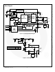
VREG 1.8V / PMID REG CREG PMID 1F PMID Q3 VBUS CMID Q1 CHARGE PUMP CBUS 1F 4.7F Q2 POWER OUTPUT STAGE Q1A PWM MODULATOR I_IN CONTROL VBUS OVP Q1B DAC COUT PGND ISNS VCC L1 1H SW RSENSE 0.1F + Battery CSIN VREF VBAT SDA SCL DISABLE OTG/USB# PMID I2C INTERFACE SYSTEM LOAD STAT 30mA CBAT OSC LOGIC AND CONTROL Figure 2.
A1 A2 A3 A4 A4 A3 A2 A1 B1 B2 B3 B4 B4 B3 B2 B1 C1 C2 C3 C4 C4 C3 C2 C1 D1 D2 D3 D4 D4 D3 D2 D1 E1 E2 E3 E4 E4 E3 E2 E1 Top View Bottom View Figure 4. WLCSP-20 Pin Assignments Pin Definitions Pin # Name Part # Description A1, A2 VBUS ALL Charger Input Voltage and USB-OTG output voltage. Bypass with a 1 F capacitor to PGND. A3 NC ALL No Connect. No external connection is made between this pin and the IC’s internal circuitry.
Stresses exceeding the absolute maximum ratings may damage the device. The device may not function or be operable above the recommended operating conditions and stressing the parts to these levels is not recommended. In addition, extended exposure to stresses above the recommended operating conditions may affect device reliability. The absolute maximum ratings are stress ratings only. Symbol Parameter VBUS VBUS Voltage VSTAT STAT Voltage VI VO dVBUS dt Min. Continuous –1.
Unless otherwise specified: according to the circuit of Figure 1; recommended operating temperature range for TJ and TA; VBUS=5.0 V; HZ_MODE; OPA_MODE=0; (Charge Mode); SCL, SDA, OTG=0 or 1.8 V; and typical values are for TJ=25°C. Symbol Parameter Conditions Min. Typ. Max.
Unless otherwise specified: according to the circuit of Figure 1; recommended operating temperature range for TJ and TA; VBUS=5.0 V; HZ_MODE; OPA_MODE=0; (Charge Mode); SCL, SDA, OTG=0 or 1.8 V; and typical values are for TJ=25°C. Symbol Parameter Conditions Min. Typ. Max. Units V Input Power Source Detection VIN(MIN)1 VBUS Input Voltage Rising To Initiate and Pass VBUS Validation 4.29 4.42 VIN(MIN)2 Minimum VBUS during Charge During Charging 3.71 3.
Unless otherwise specified: according to the circuit of Figure 1; recommended operating temperature range for TJ and TA; VBUS=5.0 V; HZ_MODE; OPA_MODE=0; (Charge Mode); SCL, SDA, OTG=0 or 1.8 V; and typical values are for TJ=25°C. Symbol Parameter Conditions Min. Typ. Max. Units 2.5 V < VBAT < 4.5 V, ILOAD from 0 to 200 mA 4.80 5.07 5.17 2.7 V < VBAT < 4.5 V, ILOAD from 0 to 200 mA 4.85 5.07 5.
Guaranteed by design. Symbol fSCL tBUF Parameter SCL Clock Frequency Bus-Free Time between STOP and START Conditions Conditions Min. tLOW START or Repeated START Hold Time SCL LOW Period 100 Fast Mode 400 High-Speed Mode, CB < 100 pF 3400 High-Speed Mode, CB < 400 pF 1700 Standard Mode 4.7 Fast Mode 1.
Guaranteed by design. Symbol Parameter tFDA Conditions SDA Fall Time tSU;STO Stop Condition Setup Time CB Min. Typ. Max. Units Standard Mode 20 + 0.1CB 300 Fast Mode 20 + 0.
180 900 160 800 140 700 Battery Charge Current (mA) Battery Charge Current (mA) Unless otherwise specified, circuit of Figure 1, VOREG=4.2 V, VBUS=5.0 V, and TA=25°C. 120 100 80 60 40 5.5VBUS 5.0VBUS 20 600 500 400 300 200 5.5VBUS 5.0VBUS 100 4.5VBUS 4.5VBUS - 2.5 3 3.5 4 4.5 2.5 3 3.5 4 4.5 Battery Voltage, VBAT (V) Figure 7. Battery Charge Current vs. VBUS with IINLIM=100 mA Figure 8. Battery Charge Current vs.
Unless otherwise specified, circuit of Figure 1, VOREG=4.2 V, VBUS=5.0 V, and TA=25°C. Figure 13. AutoCharge Startup with 300 mA Limited Charger / Adaptor, IINLIM=500 mA, OTG=1, VBAT=3.4 V Figure 14. Charger Startup with HZ_MODE Bit Reset, IINLIM=500 mA, IOCHARGE=950 mA, OREG=4.2 V, VBAT=3.6 V Figure 15. Battery Removal / Insertion during Charging, VBAT=3.9 V, IOCHARGE=950 mA, No IINLIM, TE=0 Figure 16. Battery Removal / Insertion during Charging, VBAT=3.
Unless otherwise specified, circuit of Figure 1, VOREG=4.2 V, VBUS=5.0 V, and TA=25°C. Figure 17. No Battery at VBUS Power-up; FAN5400, FAN5403 Figure 18. No Battery at VBUS Power-up; FAN5402, FAN5405 1.82 1.81 150 -30C +25C 1.80 VREG (V) High-Z Mode Current (A) 200 +85C 100 1.79 -10C, 5.0VBUS 50 1.78 +25C, 5.0VBUS +85C, 5.0VBUS 0 1.77 4.0 4.5 5.0 5.5 6.0 0 Figure 19.
100 100 95 95 Efficiency (%) Efficiency (%) Unless otherwise specified, using circuit of Figure 1, VBAT=3.6 V, TA=25°C. 90 85 2.7VBAT 80 90 85 -10C, 3.6VBAT 80 3.6VBAT +25C, 3.6VBAT 4.2VBAT +85C, 3.6VBAT 75 75 0 50 100 150 200 250 300 0 50 VBUS Load Current (mA) 100 150 200 Figure 21. Efficiency vs. VBAT 300 Figure 22. Efficiency Over-Temperature 5.12 5.12 2.7VBAT 5.09 -10C, 3.6VBAT 5.09 3.6VBAT +25C, 3.6VBAT 4.2VBAT +85C, 3.6VBAT 5.06 VBUS (V) 5.
Unless otherwise specified, using circuit of Figure 1, VBAT=3.6 V, TA=25°C. Figure 27. Boost PWM Waveform Figure 28. Boost PFM Waveform 30 30 2.7VBAT -30C, 3.6VBAT 3.6VBAT 25 +25C, 3.6VBAT 25 4.2VBAT +85C, 3.6VBAT VBUS Ripple (mVpp) VBUS Ripple (mVpp) 4.5VBAT 20 15 10 5 20 15 10 5 0 0 0 50 100 150 200 250 300 0 VBUS Load Current (mA) 100 150 200 250 300 VBUS Load Current (mA) Figure 29. Output Ripple vs.
Unless otherwise specified, using circuit of Figure 1, VBAT=3.6 V, TA=25°C. VBUS IL IBAT Figure 31. Startup, 3.6 VBAT, 44 Load, Additional 10 µF, X5R Across VBUS Figure 32. VBUS Fault Response, 3.6 VBAT Figure 33. Load Transient, 5-155-5 mA, tR=tF=100 ns Figure 34. Load Transient, 5-255-5 mA, tR=tF=100 ns © 2009 Fairchild Semiconductor Corporation FAN5400 Family • Rev. 1.10 www.fairchildsemi.
When charging batteries with a current-limited input source, such as USB, a switching charger’s high efficiency over a wide range of output voltages minimizes charging time. with a constant current if sufficient input power is available. The current slew rate is limited to prevent overshoot. The FAN540X is designed to work with a current-limited input source at VBUS.
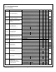
A new charge cycle begins when one of the following occurs: The battery voltage falls below VOREG - VRCH Decimal Hex VOREG VBUS Power On Reset (POR) clears and the battery voltage is below the weak battery threshold (V LOWV). This occurs for all versions except the FAN5401. CE or HZ_MODE is reset through I2C write to Decimal Hex VOREG 0 00 3.50 32 20 4.14 1 01 3.52 33 21 4.16 2 02 3.54 34 22 4.18 3 03 3.56 35 23 4.20 4 04 3.58 36 24 4.22 5 05 3.60 37 25 4.
USB-Friendly Boot Sequence The IC uses a current-mode PWM controller to regulate the output voltage and battery charge currents. The synchronous rectifier (Q2) has a negative current limit that turns off Q2 at 140 mA to prevent current flow from the battery. For all versions except FAN5401, FAN5404 At VBUS POR, when the battery voltage is above the weak battery threshold (VLOWV), the IC operates in accordance with 2 its I C register settings.
FAN5400 Family — USB-Compliant Single-Cell Li-Ion Switching Charger with USB-OTG Boost Regulator Flow Charts VBUS POR YES CE or HZ, CE# DISABLE Pin set? YES VBAT > VLOWV HZ State NO NO Charge Configuration State NO NO T15Min Timer? CE or HZ, CE# DISABLE Pin set? YES NO T32Sec Armed? YES YES CE or HZ, CE# DISABLE Pin set? YES NO HZ State T32Sec Armed? YES NO Charge State Reset all registers Start T15MIN Figure 37.
Disable Charging NO Indicate VBUS Fault VBAT < VSHORT Enable ISHORT , Reset Safety reg YES VBUS OK? NO Indicate Charging NO YES PWM Charging VBUS OK? T15MIN Timeout? YES Indicate Charging NO YES Disable Charging T15MIN Timeout? Indicate VBUS Fault Indicate timer fault YES Set CE Charge Configuration State NO NO HIGHZ mode NO IOUT < ITERM Termination enabled VBAT > VOREG–VRCH VBAT < VOREG–VRCH Indicate Charge Complete YES Reset Safety reg Delay tINT NO YES Battery Removed Stop C
FAN5400 Family — USB-Compliant Single-Cell Li-Ion Switching Charger with USB-OTG Boost Regulator Charge Configuration State T32Sec ARMED AND CE = 0? CE# YES Charge State NO Has T15Min CE = 0 and CE# NO START T15Min YES VBAT < VOREG for 262ms? NO YES Figure 39. Charge Configuration HZ State DISABLE PIN HIGH Reset T15min if running LOW Stop T32Sec RUN T32Sec NO HZ or CE# CE set? HIGH YES VBAT > VLOWV? YES NO DISABLE PIN LOW Charge State Figure 40.
Start T15MIN Reset Registers YES T32SEC NO Expired? Start T32SEC Stop T15MIN T15MIN YES Active? YES NO I2C Write received? NO Timer Fault : Set CE CE T15MIN Expired? NO Continue Charging YES Figure 41. Timer Flow Chart for FAN5400, FAN5402, FAN5403, FAN5405 Charge Start from Host control Reset T32SEC Charge T32SEC Expired? YES Timer Fault Stop Charging and Reset Registers NO NO YES TMR_RST bit Set? Figure 42.
FAN5403-05 Only The FAN5403, FAN5404, and FAN5405 have additional functionality to limit input current in case a current-limited “special charger” is supplying VBUS. The FAN5403-05 slowly increases the charging current until either: ISAFE (REG6[6:4]) DEC IINLIM or IOCHARGE is reached or VBUS=VSP. If VBUS collapses to VSP when the current is ramping up, the FAN5403-05 charge with an input current that keeps VBUS=VSP.
Battery Detection During Charging The IC can detect the presence, absence, or removal of a battery if the termination bit (TE) is set. During normal charging, once VBAT is close to VOREG and the termination charge current is detected, the IC terminates charging and sets the STAT bits to 10. It then turns on a discharge current, IDETECT, for tDETECT. If VBAT is still above VOREG – VRCH, the battery is present and the IC sets the FAULT bits to 000.
Charge Mode Control Bits 2 Setting either HZ_MODE or CE through I C disables the charger and puts the IC into High-Impedance Mode and resets t32S. If VBAT < VLOWV while in High-Impedance Mode, t32S begins running and, when it overflows, all registers (except SAFETY) reset, which enables t15MIN charging on versions with the 15-minute timer. If the system is powered up without a battery present, the CV bit should be set. When a battery is inserted, the CV bit is cleared.
Boost Mode can be enabled if the IC is in 32-Second Mode with the OTG pin and OPA_MODE bits as indicated in Table 16. The OTG pin ACTIVE state is 1 if OTG_PL=1 and 0 when OTG_PL=0. VOUT 5.07 ROUT ILOAD At VBAT=3.3 V, and ILOAD=200 mA, VBUS would drop to: If boost is active using the OTG pin, Boost Mode is initiated even if the HZ_MODE=1. The HZ_MODE bit overrides the OPA_MODE bit. VOUT 5.07 0.26 0.2 5.018V EQ. 1A At VBAT=2.7V, and ILOAD=200mA, VBUS would drop to: Table 16.
VREG Pin This is the normal operating mode of the regulator. The regulator uses a minimum tOFF-minimum tON modulation scheme. The minimum tOFF is proportional to VIN , which The VREG pin on FAN5400 - FAN5402 provides a voltage protected from over-voltage surges on VBUS, which can be used to run auxiliary circuits. This voltage is essentially a current-limited replica of PMID. The maximum voltage on this node is 5.9 V. VOUT keeps the regulator’s switching frequency reasonably constant in CCM.
BIT# STATE NAME 0 MONITOR Active When 1 Address 10h 7 ITERM_CMP 6 VBAT_CMP VCSIN – VBAT < VITERM VCSIN – VBAT > VITERM Charging with TE=1 VCSIN – VBAT < 1mV VCSIN – VBAT > 1mV Charging with TE=0 VBAT < VSHORT VBAT > VSHORT Charging VBAT < VLOWV VBAT > VLOWV High-Impedance Mode VBAT < UVLOBST VBAT > UVLOBST Boosting Charging 5 LINCHG Linear Charging Not Enabled Linear Charging Enabled 4 T_120 TJ < 120°C TJ > 120°C 3 ICHG Charging Current Controlled by ICHARGE Control Loop
The FAN540X’s serial interface is compatible with Standard, 2 Fast, Fast Plus, and High-Speed Mode I C-Bus® specifications. The FAN540X’s SCL line is an input and its SDA line is a bi-directional open-drain output; it can only pull down the bus when active. The SDA line only pulls LOW during data reads and when signaling ACK. All data is shifted in MSB (bit 7) first. Slave Releases SDA Master Drives tHD;STO ACK(0) or NACK(1) SCL Slave Address Figure 47. Stop Bit 2 Table 20.
Table 21. Bit Definitions for Figure 49, Figure 50 The figures below outline the sequences for data read and write. Bus control is signified by the shading of the packet, Master Drives Bus defined as and All addresses and data are MSB first. Slave Drives Bus 7 bits S Slave Address 0 Symbol . Definition S START, see Figure 46. A ACK. The slave drives SDA to 0 to acknowledge the preceding packet. A NACK. The slave sends a 1 to NACK the preceding packet.
The FAN5400-FAN5402 have seven user-accessible registers; the FAN5403-05 have an additional two registers, as defined in Table 22. 2 Table 22.
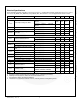
Bit Name Value Type CONTROL1 7:6 Register Address: 01 IINLIM 00 5:4 VLOWV 3 TE 2 CE 1 HZ_MODE 0 Description Input current limit, see Table 7 R/W 3.4 V 01 3.5 V 10 3.6 V 11 3.
SP_CHARGER (FAN5403 – FAN5405) 7 Reserved 6 DIS_VREG 0 R 0 R/W 1 0 5 IO_LEVEL 4 SP 3 EN_LEVEL 2:0 VSP R 1.8 V regulator is ON Output current is controlled by IOCHARGE bits Special charger is not active (VBUS is able to stay above VSP) Special charger has been detected and VBUS is being regulated to VSP R 1 Table 8 Unused Voltage across RSENSE for output current control is set to 22.1 mV (325 mA for RSENSE=68 m, 221 mA for 100 m) 1 0 Default Value=001X X100 1.
Bypass capacitors should be placed as close to the IC as possible. In particular, the total loop length for CMID should be minimized to reduce overshoot and ringing on the SW, PMID, and VBUS pins. All power and ground pins must be routed to their bypass capacitors using top copper if possible. Copper area connecting to the IC should be maximized to improve thermal performance. Figure 51.
BALL A1 INDEX AREA F A E 1.20 B A1 Cu Pad 0.03 C 1.20 A1 2X 1.60 D 0.40 Mask Opening Mask Opening 0.40 0.40 option 1 0.03 C 2X TOP VIEW Cu Pad option 2 RECOMMENDED LAND PATTERN (NSMD TYPE) 0.06 C 0.625 0.547 0.05 C E C SEATING PLANE SIDE VIEWS D 0.005 1.20 0.40 20X E D C B 1.60 0.40 A 1 2 3 4 BOTTOM VIEW F C A B NOTES: A. NO JEDEC REGISTRATION APPLIES. B. DIMENSIONS ARE IN MILLIMETERS. C. DIMENSIONS AND TOLERANCE PER ASMEY14.5M, 2009. D.
ON Semiconductor and are trademarks of Semiconductor Components Industries, LLC dba ON Semiconductor or its subsidiaries in the United States and/or other countries. ON Semiconductor owns the rights to a number of patents, trademarks, copyrights, trade secrets, and other intellectual property. A listing of ON Semiconductor’s product/patent coverage may be accessed at www.onsemi.com/site/pdf/Patent−Marking.pdf. ON Semiconductor reserves the right to make changes without further notice to any products herein.