
Data Sheet


www.onsemi.com
7
FAN3121 / FAN3122 — Single 9-A High-Speed, Low-Side Gate Driver
Symbol
Parameter
Conditions
Min.
Typ.
Max.
Unit
FAN3121-F085, FAN3122-F085 (Automotive-Qualified Ver
sions)
t
RISE
Output Rise Time
(11)
CMOS Inputs
C
LOAD
=10 nF
12
23
31
ns
t
FALL
Output Fall Time
(11)
CMOS Inputs
C
LOAD
=10 nF
12
19
27
ns
t
RISE
Output Rise Time
(11)
TTL Inputs
C
LOAD
=10 nF
18
23
36
ns
t
FALL
Output Fall Time
(11)
TTL Inputs
C
LOAD
=10 nF
10
19
28
ns
t
D1,
t
D2
Output Propagation Delay, CMOS Inputs
(13)
0 – 12 V
IN
, 1 V/ns Slew Rate
6
18
35
ns
t
D1,
t
D2
Output Propagation Delay, TTL Inputs
(11)
0 – 5 V
IN
, 1 V/ns Slew Rate
9
23
36
ns
V
OH
High Level Output Voltage
(13)
VOH=VDD–VOUT, IOUT=–1 mA
15
35
mV
V
OL
Low Level Output Voltage
(13)
IOUT=1 mA
10
25
mV
Notes:
9. Lower supply current due to inactive TTL circuitry.
10. EN inputs have modified TTL thresholds; refer to the ENABLE section.
11. See Timing Diagrams of Figure 8 and Figure 9.
12. Not tested in production.
13. Automotive-qualified F085 version specifications.
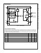
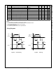
Timing Diagrams
t
D1
t
D2
t
FALL
t
RISE
V
IL
V
IH
Input
or
Enable
90%
10%
Output
t
D1
t
D2
t
FALL
t
RISE
V
IL
V
IH
Input
or
Enable
90%
10%
Output
Figure 8. Non-Inverting
Figure 9. Inverting