
Data Sheet


www.onsemi.com
5
FAN3121 / FAN3122 — Single 9-A High-Speed, Low-Side Gate Driver
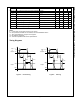
Recommended Operating Conditions
The Recommended Operating Conditions table defines the conditions for actual device operation. Recommended
operating conditions are specified to ensure optimal performance to the datasheet specifications. ON Semiconductor
does not recommend exceeding them or designing to Absolute Maximum Ratings.
Symbol
Parameter
Min.
Max.
Unit
V
DD
Supply Voltage Range
4.5
18.0
V
V
EN
Enable Voltage EN
0
V
DD
V
V
IN
Input Voltage IN
0
V
DD
V
T
A
Operating Ambient Temperature
-40
+125
ºC
Electrical Characteristics
Unless otherwise noted, V
DD
=12 V and T
J
=-40°C to +125°C. Currents are defined as positive into the device and
negative out of the device.
Symbol
Parameter
Conditions
Min.
Typ.
Max.
Unit
Supply
V
DD
Operating Range
4.5
18.0
V
I
DD
Supply Current, Inputs / EN Not Connected
TTL
0.65
0.90
mA
CMOS
(9)
0.58
0.85
V
ON
Device Turn-On Voltage (UVLO)
3.5
4.0
4.3
V
V
OFF
Device Turn-Off Voltage (UVLO)
3.30
3.75
4.10
V
FAN3121-F085, FAN3122-F085 (Automotive-Qualified Ver
sions)
V
DD
Operating Range
4.5
18.0
V
I
DD
Supply Current, Inputs / EN Not Connected
TTL
0.65
1.00
mA
CMOS
(9)
0.58
0.85
V
ON
Device Turn-On Voltage (UVLO)
3.5
4.0
4.3
V
V
OFF
Device Turn-Off Voltage (UVLO)
(13)
3.25
3.75
4.15
V
Inputs (TTL, FAN312xT)
(10)
V
IL_T
INx Logic Low Threshold
0.8
1.0
V
V
IH_T
INx Logic High Threshold
1.7
2.0
V
V
HYS_T
TTL Logic Hysteresis Voltage
0.40
0.70
0.85
V
FAN3121TMX, FAN3122TMX
I
IN+
Non-Inverting Input Current
IN from 0 to V
DD
-1
175
µA
I
IN-
Inverting Input Current
IN from 0 to V
DD
-175
1
µA
FAN3121TMX-F085, FAN3122TMX-F085 (Autom
otive-Qualified Versions)
I
INx_T
Non-inverting Input Current
(13)
IN=0 V
-1.5
1.5
µA
I
INx_T
Non-inverting Input Current
(13)
IN=V
DD
90
120
175
µA
I
INx_T
Inverting Input Current
(13)
IN=0 V
-175
-120
-90
µA
I
INx_T
Inverting Input Current
(13)
IN=V
DD
-1.5
1.5
µA