
Data Sheet


www.onsemi.com
4
FAN3121 / FAN3122 — Single 9-A High-Speed, Low-Side Gate Driver
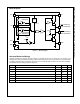
Block Diagram
Figure 7. Block Diagram
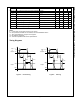
Absolute Maximum Ratings
Stresses exceeding the absolute maximum ratings may damage the device. The device may not function or be
operable above the recommended operating conditions and stressing the parts to these levels is not recommended.
In addition, extended exposure to stresses above the recommended operating conditions may affect device reliability.
The absolute maximum ratings are stress ratings only.
Symbol
Parameter
Min.
Max.
Unit
V
DD
V
DD
to GND
-0.3
20.0
V
V
EN
EN to GND
GND - 0.3
V
DD
+ 0.3
V
V
IN
IN to GND
GND - 0.3
V
DD
+ 0.3
V
V
OUT
OUT to GND
GND - 0.3
V
DD
+ 0.3
V
T
L
Lead Soldering Temperature (10 Seconds)
+260
°C
T
J
Junction Temperature
-55
+150
°C
T
STG
Storage Temperature
-65
+150
°C
EN
3
8
V
DD
6
5
GND
UVLO
V
DD_OK
IN
2
100k
100k
100k
V
DD
Inverting
(FAN3121)
Non-Inverting
(FAN3122)
7
V
DD
1
4
GND
OUT (FAN3122)
OUT (FAN3121)
OUT (FAN3122)
OUT (FAN3121)
100k