
Data Sheet
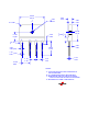


DFB2005 - DFB20100 — Glass-Passivated Bridge Rectifiers
© 2009 Fairchild Semiconductor Corporation www.fairchildsemi.com
DFB2005 - DFB20100 Rev. 1.2.2 2
Absolute Maximum Ratings
(1)
Stresses exceeding the absolute maximum ratings may damage the device. The device may not function or be opera-
ble above the recommended operating conditions and stressing the parts to these levels is not recommended. In addi-
tion, extended exposure to stresses above the recommended operating conditions may affect device reliability. The
absolute maximum ratings are stress ratings only. Values are at T
A
= 25°C unless otherwise noted.
Notes:
1. Single-phase, half-wave, 60 Hz, resistive or inductive load. For capacitive load, derate current by 20%.
2. Device mounted on 4 inch x 5 inch x 0.25 inch Al-plate heat sink.
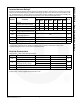
Electrical Characteristics
Values are at T
A
= 25°C unless otherwise specified.
Note:
3. Measured at 1 MHz and applied reverse bias of 4.0 V DC.
Symbol Parameter
Value
Units
DFB
2005
DFB
2010
DFB
2020
DFB
2040
DFB
2060
DFB
2080
DFB
20100
V
RRM
Maximum
Recurrent Peak Reverse Voltage
50 100 200 400 600 800 1000 V
V
RMS
Maximum RMS Voltage 35 70 140 280 420 560 700 V
V
DC
Maximum DC Blocking Voltage 50 100 200 400 600 800 1000 V
I
(AV)
Maximum
Average Forward Rectified Current
20 A
I
FSM
Peak Forward Surge Current
(8.3 ms Single Half-wave)
250 A
R
θJC
Typical Thermal Resistance
(2)
4.75 °C/W
T
J
Operating Temperature Range -55 to +150 °C
T
STG
Storage Temperature Range -55 to +150 °C
Symbol Parameter Test condition Value Unit
V
F
Maximum 10 A 1.0
V
Instantaneous Forward Voltage 20 A 1.1
I
R
Maximum DC Reverse Current
at Rated DC Blocking Voltage
T
A
= 25°C 10
μA
T
A
= 125°C 500
I
2
t Rating for Fusing (t < 8.3 ms) 259 A
2
s
C
J
Typical Junction Capacitance per Leg
(3)
140 pF