
Data Sheet


NPN Switching Transistor
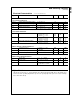
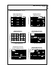
Absolute Maximum Ratings* TA = 25°C unless otherwise noted
*These ratings are limiting values above which the serviceability of any semiconductor device may be impaired.
NOTES:
1) These ratings are based on a maximum junction temperature of 150 degrees C.
2) These are steady state limits. The factory should be consulted on applications involving pulsed or low duty cycle operations.
Thermal Characteristics TA = 25°C unless otherwise noted
BSV52
This device is designed for high speed saturated switching at
collector currents of 10 mA to 100 mA. Sourced from Process 21.
Symbol Parameter Value Units
V
CEO
Collector-Emitter Voltage 12 V
V
CES
Collector-Base Voltage 20 V
V
EBO
Emitter-Base Voltage 5.0 V
I
C
Collector Current - Continuous 200 mA
T
J
, T
stg
Operating and Storage Junction Temperature Range -55 to +150
°
C
Symbol Characteristic Max Units
*BSV52
P
D
Total Device Dissipation
Derate above 25
°
C
225
1.8
mW
mW/
°
C
R
θ
JA
Thermal Resistance, Junction to Ambient 556
°
C/W
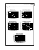
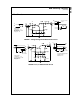
C
E
B
SOT-23
Mark: B2
*Device mounted on FR-4 PCB 40 mm X 40 mm X 1.5 mm.
1997 Fairchild Semiconductor Corporation
BSV52