
Data Sheet
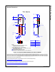
BD135 / 137 / 139 — Features
© 2007 Fairchild Semiconductor Corporation www.fairchildsemi.com
BD135 / 137 / 139 Rev. 1.2.0 2
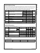
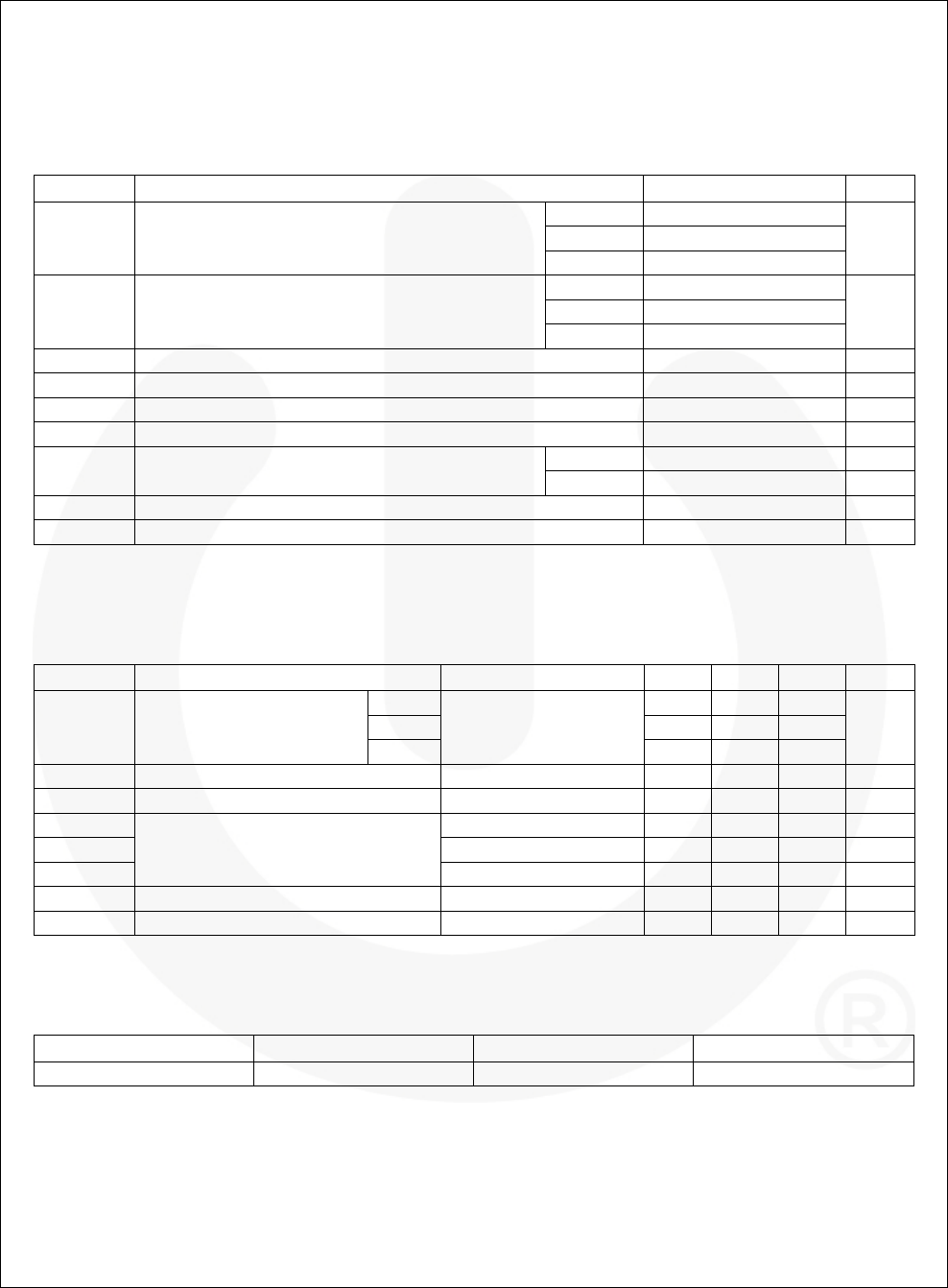
Absolute Maximum Ratings
Stresses exceeding the absolute maximum ratings may damage the device. The device may not function or be opera-
ble above the recommended operating conditions and stressing the parts to these levels is not recommended. In addi-
tion, extended exposure to stresses above the recommended operating conditions may affect device reliability. The
absolute maximum ratings are stress ratings only. Values are at T
C
= 25°C unless otherwise noted.
Electrical Characteristics
Values are at T
C
= 25°C unless otherwise noted.
h
FE
Classification
Symbol Parameter Value Units
V
CBO
Collector-Base Voltage
BD135 45
VBD137 60
BD139 80
V
CEO
Collector-Emitter Voltage
BD135 45
VBD137 60
BD139 80
V
EBO
Emitter-Base Voltage 5 V
I
C
Collector Current (DC) 1.5 A
I
CP
Collector Current (Pulse) 3.0 A
I
B
Base Current 0.5 A
P
C
Device Dissipation
T
C
= 25°C12.5 W
T
A
= 25°C1.25 W
T
J
Junction Temperature 150 °C
T
STG
Storage Temperature - 55 to +150 °C
Symbol Parameter Test Condition Min. Typ. Max. Units
V
CEO
(sus)
Collector-Emitter Sustaining
Voltage
BD135
I
C
= 30 mA, I
B
= 0
45
VBD137 60
BD139 80
I
CBO
Collector Cut-off Current V
CB
= 30 V, I
E
= 0 0.1 μA
I
EBO
Emitter Cut-off Current V
EB
= 5 V, I
C
= 0 10 μA
h
FE1
DC Current Gain
V
CE
= 2 V, I
C
= 5 mA 25
h
FE2
V
CE
= 2 V, I
C
= 0.5 A 25
h
FE3
V
CE
= 2 V, I
C
= 150 mA 40 250
V
CE
(sat) Collector-Emitter Saturation Voltage I
C
= 500 mA, I
B
= 50 mA 0.5 V
V
BE
(on) Base-Emitter On Voltage V
CE
= 2 V, I
C
= 0.5 A 1 V
Classification 6 10 16
h
FE3
40 ~ 100 63 ~ 160 100 ~ 250