
Data Sheet

© Semiconductor Components Industries, LLC, 2011
June, 2011 − Rev. 1
1 Publication Order Number:
BC640/D
BC640-016G
High Current Transistors
PNP Silicon
Features
• This is a Pb−Free Device
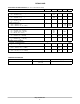
MAXIMUM RATINGS
Rating Symbol Value Unit
Collector-Emitter Voltage V
CEO
−80 Vdc
Collector-Base Voltage V
CBO
−80 Vdc
Emitter-Base Voltage V
EBO
−5.0 Vdc
Collector Current − Continuous I
C
−0.5 Adc
Total Device Dissipation @ T
A
= 25°C
Derate above 25°C
P
D
625
5.0
mW
mW/°C
Total Device Dissipation @ T
C
= 25°C
Derate above 25°C
P
D
1.5
12
W
mW/°C
Operating and Storage Junction
Temperature Range
T
J
, T
stg
−55 to +150 °C
THERMAL CHARACTERISTICS
Characteristic Symbol Max Unit
Thermal Resistance, Junction−to−Ambient
R
q
JA
200 °C/W
Thermal Resistance, Junction−to−Case
R
q
JC
83.3 °C/W
Stresses exceeding Maximum Ratings may damage the device. Maximum
Ratings are stress ratings only. Functional operation above the Recommended
Operating Conditions is not implied. Extended exposure to stresses above the
Recommended Operating Conditions may affect device reliability.
*For additional information on our Pb−Free strategy and soldering details, please
download the ON Semiconductor Soldering and Mounting Techniques
Reference Manual, SOLDERRM/D.
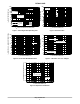
COLLECTOR
2
3
BASE
1
EMITTER
See detailed ordering and shipping information in the package
dimensions section on page 2 of this data sheet.
ORDERING INFORMATION
http://onsemi.com
1
2
3
STRAIGHT LEAD
BULK PACK
TO−92
CASE 29
STYLE 14
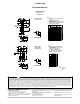
MARKING DIAGRAMS
BC64
0−16
AYWW G
G
A = Assembly Location
Y = Year
WW = Work Week
G = Pb−Free Package
(Note: Microdot may be in either location)