
Data Sheet


74VHC373 Octal D-Type Latch with 3-STATE Outputs
©1993 Fairchild Semiconductor Corporation www.fairchildsemi.com
74VHC373 Rev. 1.3 5
AC Electrical Characteristics
Notes:
3. Parameter guaranteed by design. t
OSLH
= |t
PLH max
– t
PLH min
|; t
OSHL
= |t
PHL max
– t
PHL
min|
4. C
PD
is defined as the value of the internal equivalent capacitance which is calculated from the operating
current consumption without load. Average operating current can be obtained by the equation:
I
CC
(opr.) = C
PD
• V
CC
• f
IN
+ I
CC
/8 (per Latch). The total C
PD
when n pcs. of the Latch operates can be
calculated by the equation: C
PD
(total) = 14 + 13n.
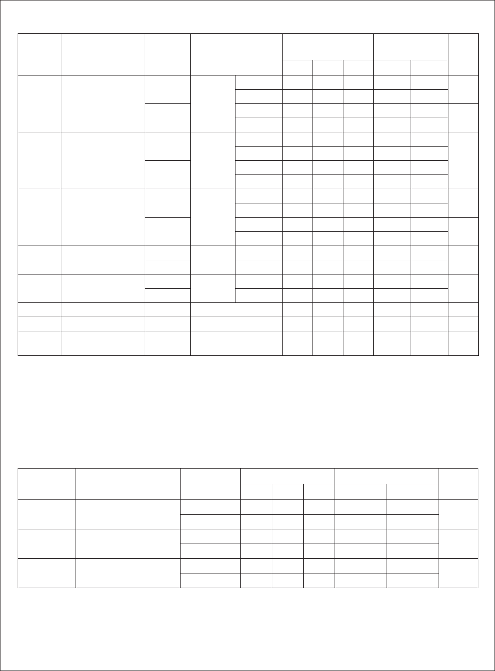
AC Operating Requirements
Symbol Parameter V
CC
(V) Conditions
T
A
= +25°C
T
A
= –40°C to
+85°C
UnitsMin. Typ. Max. Min. Max.
t
PLH
, t
PHL
Propagation Delay
Time (LE to O
n
)
3.3 ± 0.3 C
L
= 15pF 7.0 11.0 1.0 13.0 ns
C
L
= 50pF 9.5 14.5 1.0 16.5
5.0 ± 0.5 C
L
= 15pF 4.9 7.2 1.0 8.5 ns
C
L
= 50pF 6.4 9.2 1.0 10.5
t
PLH
, t
PHL
Propagation Delay
Time (D to O
n
)
3.3 ± 0.3 C
L
= 15pF 7.3 11.4 1.0 13.5 ns
C
L
= 50pF 9.8 14.9 1.0 17.0
5.0 ± 0.5 C
L
= 15pF 5.0 7.2 1.0 8.5
C
L
= 50pF 6.5 9.2 1.0 10.5
t
PZL
, t
PZH
3-STATE Output
Enable Time
3.3 ± 0.3 R
L
= 1kΩ C
L
= 15pF 7.3 11.4 1.0 13.5 ns
C
L
= 50pF 9.8 14.9 1.0 17.0
5.0 ± 0.5 C
L
= 15pF 5.5 8.1 1.0 9.5 ns
C
L
= 50pF 7.0 10.1 1.0 11.5
t
PLZ
, t
PHZ
3-STATE Output
Disable Time
3.3 ± 0.3 R
L
= 1kΩ C
L
= 50pF 9.5 13.2 1.0 15.0 ns
5.0 ± 0.5 C
L
= 50pF 6.5 9.2 1.0 10.5
t
OSLH
,
t
OSHL
Output to Output
Skew
3.3 ± 0.3
(3)
C
L
= 50pF 1.5 1.5 ns
5.0 ± 0.5 C
L
= 50pF 1.0 1.0
C
IN
Input Capacitance V
CC
= Open 4 10 10 pF
C
OUT
Output Capacitance V
CC
= 5.0V 6 pF
C
PD
Power Dissipation
Capacitance
(4)
27 pF
Symbol Parameter V
CC
(V)
T
A
= +25°C T
A
= –40°C to +85°C
UnitsMin. Typ. Max. Min. Max.
t
W
(H) Minimum Pulse Width
(LE)
3.3 ± 0.3 5.0 5.0 ns
5.0 ± 0.5 5.0 5.0
t
S
Minimum Set-Up Time 3.3 ± 0.3 4.0 4.0 ns
5.0 ± 0.5 4.0 4.0
t
H
Minimum Hold Time 3.3 ± 0.3 1.0 1.0 ns
5.0 ± 0.5 1.0 1.0