
Data Sheet


©1995 Fairchild Semiconductor Corporation www.fairchildsemi.com
74LCX125 Rev. 1.7.1 2
74LCX125 — Low Voltage Quad Buffer with 5V Tolerant Inputs and Outputs
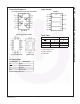
Connection Diagrams
Pin Assignments for SOIC, SOP, and TSSOP
(Top View)
Pad Assignments for DQFN
(Top Through View)
Pin Description
Logic Symbol
IEEE/IEC
Truth Table
H
=
HIGH Voltage Level
L
=
LOW Voltage Level
Z
=
High Impedance
X
=
Immaterial
Pin Names Description
A
n
Inputs
OE
n
Output Enable Inputs
O
n
Outputs
Inputs Output
OE
n
A
n
O
n
LLL
LHH
HXZ
(Bottom View)
DAP
No Connect
Note: DAP (Die Attach Pad)