
Data Sheet


74LCX125 — Low Voltage Quad Buffer with 5V Tolerant Inputs and Outputs
©1995 Fairchild Semiconductor Corporation www.fairchildsemi.com
74LCX125 Rev. 1.7.1
74LCX125
Low Voltage Quad Buffer with 5V Tolerant
Inputs and Outputs
Features
■
5V tolerant inputs and outputs
■
2.3V–3.6V V
CC
specifications provided
■
6.0ns t
PD
max. (V
CC
=
3.3V), 10µA I
CC
max.
■
Power down high impedance inputs and outputs
■
Supports live insertion/withdrawal
(1)
■
±24mA output drive (V
CC
=
3.0V)
■
■
Latch-up performance exceeds JEDEC 78 conditions
■
ESD performance:
– Human body model
>
2000V
– Machine model
>
100V
■
Leadless DQFN package
Note:
1. To ensure the high-impedance state during power up
or down, OE should be tied to V
CC
through a pull-up
resistor: the minimum value of the resistor is
determined by the current-sourcing capability of the
driver.
General Description
The LCX125 contains four independent non-inverting
buffers with 3-STATE outputs. The inputs tolerate volt-
ages up to 7V allowing the interface of 5V systems to 3V
systems.
The 74LCX125 is fabricated with an advanced CMOS
technology to achieve high speed operation while main-
taining CMOS low power dissipation.
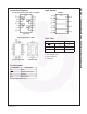
Ordering Information
Note:
2. DQFN package available in Tape and Reel only.
Device also available in Tape and Reel. Specify by appending suffix letter “X” to the ordering number.
All packages are lead free per JEDEC: J-STD-020B standard.
Order Number
Package
Number Package Description
74LCX125M M14A 14-Lead Small Outline Integrated Circuit (SOIC), JEDEC MS-012, 0.150" Narrow
74LCX125SJ M14D 14-Lead Small Outline Package (SOP), EIAJ TYPE II, 5.3mm Wide
74LCX125BQX
(2)
MLP14A 14-Terminal Depopulated Quad Very-Thin Flat Pack No Leads (DQFN), JEDEC
MO-241, 2.5 x 3.0mm
74LCX125MTC MTC14 14-Lead Thin Shrink Small Outline Package (TSSOP), JEDEC MO-153, 4.4mm
Wide
Implements
proprietary
noise/EMI reduction circuitry
December 2013