
Data Sheet

2N7000 / 2N7002 / NDS7002A — N-Channel Enhancement Mode Field Effect Transistor
www.onsemi.com
2
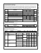
Absolute Maximum Ratings
Stresses exceeding the absolute maximum ratings may damage the device. The device may not function or be opera-
ble above the recommended operating conditions and stressing the parts to these levels is not recommended. In addi-
tion, extended exposure to stresses above the recommended operating conditions may affect device reliability. The
absolute maximum ratings are stress ratings only. Values are at T
C
= 25°C unless otherwise noted.
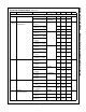
Thermal Characteristics
Values are at T
C
= 25°C unless otherwise noted.
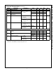
Electrical Characteristics
Values are at T
C
= 25°C unless otherwise noted.
Symbol Parameter
Value
Unit
2N7000 2N7002 NDS7002A
V
DSS
Drain-to-Source Voltage 60 V
V
DGR
Drain-Gate Voltage (R
GS
≤ 1 M 60 V
V
GSS
Gate-Source Voltage - Continuous ±20 V
Gate-Source Voltage - Non Repetitive (tp < 50 S) ±40
I
D
Maximum Drain Current - Continuous 200 115 280 mA
Maximum Drain Current - Pulsed 500 800 1500
P
D
Maximum Power Dissipation Derated above 25°C 400 200 300 mW
3.2 1.6 2.4 mW/°C
T
J,
T
STG
Operating and Storage Temperature Range
-55 to 150 -65 to 150 °C
T
L
Maximum Lead Temperature for Soldering Purposes,
1/16-inch from Case for 10 Seconds
300 °C
Symbol Parameter
Value
Unit
2N7000 2N7002 NDS7002A
R
JA
Thermal Resistance, Junction to Ambient
312.5 625 417 °C/W
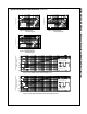
Symbol Parameter Conditions Type Min. Typ. Max. Unit
Off Characteristics
BV
DSS
Drain-Source Breakdown
Voltage
V
GS
= 0 V, I
D
= 10 AAll 60 V
I
DSS
Zero Gate Voltage Drain
Current
V
DS
= 48 V, V
GS
= 0 V 2N7000 1 A
V
DS
= 48 V, V
GS
= 0 V,
T
C
= 125°C
1
mA
V
DS
= 60 V, V
GS
= 0 V 2N7002
NDS7002A
1 A
V
DS
= 60 V, V
GS
= 0 V,
T
C
= 125°C
0.5
mA
I
GSSF
Gate - Body Leakage,
Forward
V
GS
= 15 V, V
DS
= 0 V 2N7000
10 nA
V
GS
= 20 V, V
DS
= 0 V 2N7002
NDS7002A
100 nA
I
GSSR
Gate - Body Leakage,
Reverse
V
GS
= -15 V, V
DS
= 0 V 2N7000
-10 nA
V
GS
= -20 V, V
DS
= 0 V 2N7002
NDS7002A
-100 nA