
Data Sheet

1N4728A - 1N4758A — Zener Diodes
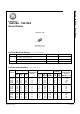
Top Mark Information (Continued)
General Requirements:
1.0 Cathode Band
2.0 First Line: - ON Semiconductor Logo
3.0 Second Line: Device name - For 1Nxx series: 3
rd
to 4
th
characters of the device name.
For BZxx series: 4
th
to 6
th
characters of the device name.
4.0 Third Line: Device name - For 1Nxx series: 5
th
to 6
th
characters of the device name.
For BZXyy series: Voltage rating
5.0 Third Line: Device name - For 1Nxx series: 7
th
to 8
th
characters of the device name.
(the 8th character is the large die identification)
For BZXyy series: Large Die Identification character
6.0 Fourth Line: Date Code - Two Digit - Six Weeks Date Code
Where: X represents the last digit of the calendar year
Y represents the Six weeks numeric code
7.0 Devices shall be marked as required in the device specification (PID or ON Semiconductor Test Spec).
8.0 Maximum no. of marking lines: 5
9.0 Maximum no. of digits per line: 3
10.0 ON Semiconductor logo must be 20 % taller than the alphanumeric marking and should occupy the 2 characters of the
specified line. 11.0 Marking Font: Arial (Except ON Semiconductor Logo)
12.0 First character of each marking line must be aligned vertically.
13.0 All device markings must be based on ON Semiconductor device specification.
47
36
A
1
st
line: F - ON Semiconductor Logo
2
nd
line: Device Name - 3
rd
to 4
th
characters of device name for 1Nxx series
or 4
th
to 6
th
characters for BZXyy series
3
rd
line: Device Name - 5
th
to 6
th
characters of device name for 1Nxx series
or Voltage rating for BZXyy series
4
th
line: Device Name - 7
th
to 8
th
characters of device name for 1Nxx series
or Large Die identification only for BZXyy series
5
th
line: Date Code - Two Digit - Six Weeks Date Code
www.onsemi.com
3
XY