
Datasheet

CJ1W-OC/OA/OD
20
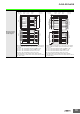
CJ1W-OD202 Transistor Output Unit (8 Points)
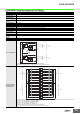
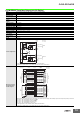
* Terminal numbers A0 to A8 and B0 to B8 are used in the external connection and terminal-device variable diagrams. They are not printed on
the Units.
Note: Although 16 I/O bits (1 word) are allocated, only 8 of these can be used for external I/O.
Name 8-point Transistor Output Unit with Terminal Block (Sourcing Outputs)
Model CJ1W-OD202
Rated Voltage 24 VDC
Operating Load
Voltage Range
20.4 to 26.4 VDC
Maximum Load
Current
2 A/point, 8 A/Unit
Leakage Current 0.1 mA max.
Residual Voltage 1.5 V max.
ON Response Time 0.5 ms max.
OFF Response Time 1.0 ms max.
Load Short-circuit
Protection
Detection current: 6 A min.
Automatic restart after error clearance.
Line Disconnection
Detection
Detection current: 200 mA
Insulation Resistance
20 MΩ between the external terminals and the GR terminal (100 VDC)
Dielectric Strength 1,000 VAC between the external terminals and the GR terminal for 1 minute at a leakage current of 10 mA max.
Number of Circuits 8 (4 points/common, 2 circuits)
Internal Current
Consumption
110 mA max.
Fuse None
External Power
Supply
24 VDC, 50 mA min.
Weight 120 g max.
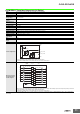
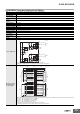
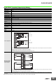
Circuit Configuration
• When overcurrent or line disconnection is detected, the ERR indicator will light, and the corresponding bit (two points per bit) in the Basic
I/O Unit Information Area (A050 to A069) will change to TRUE.
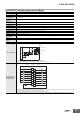
• The signal names of the terminals are the device variable names.
The device variable names are the names that use "Jxx" as the device name.
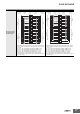
External connection
and terminal-device
variable diagram
• When wiring, pay careful attention to the polarity of the external power supply. The load may operate incorrectly if the polarity is reversed.
• The signal names of the terminals are the device variable names.
The device variable names are the names that use "Jxx" as the device name.
COM0 (+V)
COM1 (+V)
to
to
Output indicator
ERR indicator
Internal circuits
Signal name
Jxx_Ch1_Out03
Jxx_Ch1_Out00
0 V
Jxx_Ch1_Out04
Jxx_Ch1_Out07
0 V
Short-circuit
protection
Short-circuit
protection
24 VDC
24 VDC
Signal
name
Signal
name
Connec-
tor pin
*
B0
B1
B2
B3
B4
B5
B6
B7
B8
A0
A1
A2
A3
A4
A5
A6
A7
A8
L
L
L
L
L
L
L
L
Jxx_Ch1_Out00
Jxx_Ch1_Out02
0 V
NC
NC
Jxx_Ch1_Out04
Jxx_Ch1_Out06
NC
Jxx_Ch1_Out01
Jxx_Ch1_Out03
COM0 (+V)
NC
NC
NC
Jxx_Ch1_Out05
Jxx_Ch1_Out07
0 V
COM1 (+V)