
Datasheet


CJ1W-ID/IA
8
CJ1W-ID212 DC Input Unit (24 VDC, 16 Points)
*1. The ON response time will be 15 μs maximum and OFF response time will be 90 μs maximum even if the response time are set to 0 ms due
to internal element delays.
*2. Terminal numbers A0 to A8 and B0 to B8 are used in the external connection and terminal-device variable diagrams. They are not printed on
the Units.
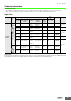
Name 16-point DC Input Unit with Terminal Block
Model CJ1W-ID212
Rated Input Voltage 24 VDC
Rated Input Voltage
Range
20.4 to 26.4 VDC
Input Impedance 3.3 kΩ
Input Current 7 mA typical (at 24 VDC)
ON Voltage/ON Current 14.4 VDC min./3 mA min.
OFF Voltage/OFF
Current
5 VDC max./1 mA max.
ON Response Time
8.0 ms max.
(Can be set to between 0 and 32 ms in the Setup.) *1
OFF Response Time
8.0 ms max.
(Can be set to between 0 and 32 ms in the Setup.) *1
Number of Circuits 16 (16 points/common, 1 circuit)
Number of
Simultaneously ON
Points
100% simultaneously ON (at 24 VDC)
(Refer to the following illustration.)
Insulation Resistance 20 MΩ min. between external terminals and the GR terminal (100 VDC)
Dielectric Strength 1,000 VAC between the external terminals and the GR terminal for 1 minute at a leakage current of 10 mA max.
Internal Current
Consumption
130 mA max.
Weight 110 g max.
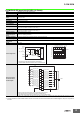
Circuit Configuration
•
The signal names of the terminals are the device variable names.
The device variable names are the names that use "Jxx" as the device name.
External connection
and terminal-device
variable diagram
• Polarity of the input power supply can be connected in either direction.
• The signal names of the terminals are the device variable names.
The device variable names are the names that use "Jxx" as the device name.
1000 pF
470
Ω
3.3 k
Ω
Internal circuits
Input indicator
to
Signal
name
Jxx_Ch1_In00
Jxx_Ch1_In15
COM
COM
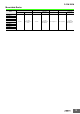
18
16
14
12
10
8
6
4
2
0
0 10 20 30 40 50 60
No. of simultaneously ON points
Input voltage: 26.4 VDC
12 points
at 55°C.
16 points
at 45°C.
Ambient temperature
(°C)
Temperature characteristics
for simultaneously ON points
B1
Jxx_Ch1_In01
B2
Jxx_Ch1_In03
B3
Jxx_Ch1_In05
B4
Jxx_Ch1_In07
B5
Jxx_Ch1_In09
B6
Jxx_Ch1_In11
B7
Jxx_Ch1_In13
B8
Jxx_Ch1_In15
COM
A1
Jxx_Ch1_In00
A2
Jxx_Ch1_In02
A3
Jxx_Ch1_In04
A4
Jxx_Ch1_In06
A5
Jxx_Ch1_In08
A6
Jxx_Ch1_In10
A7
Jxx_Ch1_In12
A8
Jxx_Ch1_In14
COM
B0
A0
24 VDC
Signal
name
Signal
name
Connector
pin
*2