
Datasheet


CJ1W-ID/IA
14
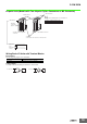
CJ1W-IA201 AC Input Unit (200 VAC, 8 Points)
*1. Can be set to 0 ms, 0.5 ms, 1 ms, 2 ms, 4 ms, 8 ms, 16 ms, or 32ms in the settings. When the response times have been set to 0 ms, the ON
response time will be 10 ms maximum and the OFF response time will be 55 ms maximum due to internal element delays.
*2. Terminal numbers A0 to A8 and B0 to B8 are used in the external connection and terminal-device variable diagrams. They are not printed on
the Units.
Note: Although 16 I/O bits (1 word) are allocated, only 8 of these can be used for external I/O.
Name 8-point AC Input Unit with Terminal Block
Model CJ1W-IA201
Rated Input Voltage 200 to 240 VAC 50/60 Hz
Rated Input Voltage
Range
170 to 264 VAC
Input Impedance 21 kΩ (50 Hz), 18 kΩ (60 Hz)
Input Current
9 mA typical (at 200 VAC, 50 Hz),
11 mA typical (at 200 VAC, 60 Hz)
ON Voltage/ON Current 120 VAC min./4 mA min.
OFF Voltage/OFF
Current
40 VAC max./2 mA max.
ON Response Time 18.0 ms max. (default setting: 8 ms) *1
OFF Response Time 48.0 ms max. (default setting: 8 ms) *1
Number of Circuits 8 (8 points/common, 1 circuit)
Number of
Simultaneously ON
Points
100% (8 points/common) simultaneously ON
Insulation Resistance 20 MΩ min. between external terminals and the GR terminal (500 VDC)
Dielectric Strength 2,000 VAC between the external terminals and the GR terminal for 1 minute at a leakage current of 10 mA max.
Internal Current
Consumption
80 mA max.
Weight 130 g max.
Accessories None
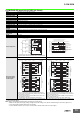
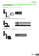
Circuit Configuration
• The signal names of the terminals are the device variable names.
The device variable names are the names that use "Jxx" as the device name.
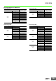
External connection
and terminal-device
variable diagram
• The signal names of the terminals are the device variable names.
The device variable names are the names that use "Jxx" as the device name.
820 Ω
1 MΩ
0.15 μF
220 Ω
Input indicator
Internal circuits
to
Signal
name
COM
Jxx_Ch1_In00
Jxx_Ch1_In07
200 to 240 VAC
Signal
name
Connec-
tor pin
*2
Jxx_Ch1_In00
Jxx_Ch1_In01
Jxx_Ch1_In02
Jxx_Ch1_In03
Jxx_Ch1_In05
Jxx_Ch1_In06
Jxx_Ch1_In07
B0
B1
B2
B3
B4
B5
B6
B7
B8
Jxx_Ch1_In04
A0
A1
A2
A3
A4
A5
A6
A7
A8
COM
NC
NC
NC
NC
NC
NC
NC
NC
NC