
User Manual
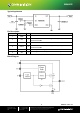
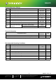
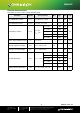
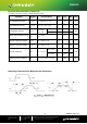
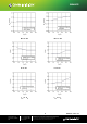
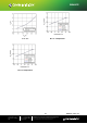
Table Of Contents

4275 Burton Drive
Santa Clara, CA 95054
USA
Tel: + 1 408 567 3000
Fax: + 1 408 567 3001
www.ovt.com
OMNIVISION reserves the right to make changes to their products or to discontinue
any product or service without further notice. OMNIVISION and the OMNIVISION logo
are trademarks or registered trademarks of OmniVision Technologies, Inc.
All other trademarks are the property of their respective owners.
4
Absolute Maximum Ratings
Symbol
Parameter
Value
Unit
V
IN
Input voltage range
-0.3
~
5.5
V
V
OUT
Output voltage range
-0.3~5.5
V
V
BIAS
Bias voltage range
-0.3~5.5
V
V
ON
Input voltage range
-0.3
~
5.5
V
I
MAX
Maximum continuous switch current
4.5
A
T
JMAX
Maximum junction temperature
150
°C
T
STG
Storage temperature range
-60~150
°C
T
LEAD
Maximum lead temperature (10-s soldering time)
260
°C
ESD
Electrostatic discharge
protection
Human-Body Model (HBM)
±2000
V
Charged-Device Model (CDM)
±1000
Thermal Information
Thermal Resistance
WS4667E
SOT23-6L
Unit
Thermal Resistance, R
θJA
(Junction-to-Ambient)Without Copper Pour
198
°C/W
Thermal Resistance, R
θJA
(Junction-to-Ambient)With Copper Pour*
133
°C/W
*:Surface mounted on FR-4 Board using 2 oz, 1 square inch Cu area, PCB board size 1.5*1.5 square inches.
Recommended Operating Conditions
Symbol
Parameter
Value
Unit
V
IN
Input voltage range
0.8~V
BIAS
–2
V
V
BIAS
Bias voltage range
3~5.5
V
V
ON
ON voltage range
0~5.5
V
V
OUT
Output voltage range
0~V
IN
V
T
J
Junction temperature range
-40~125
°C
T
A
Ambient temperature range
0~85
°C
C
IN
Input capacitor
1
μF
C
L
Output capacitor
0.1
μF
WS4667E
2022/1/4 - Rev. 0.5