
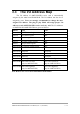
- OMEGA Engineering, Inc. PCI-Bus Digital I/O Board Product Manual
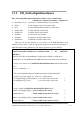
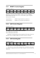


3.3.4 INT Mask Control Register
(Read/Write): wBase+5
Bit 7 Bit 6 Bit 5 Bit 4 Bit 3 Bit 2 Bit 1 Bit 0
0 0 0 0 EN3 EN2 EN1 EN0
Note. Refer to Sec. 3.1 for more information about wBase.
EN0=0Æ disable PC0 as a interrupt signal (default)
EN0=1Æ enable PC0 as a interrupt signal
outportb(wBase+5,0); /* disable interrupt */
outportb(wBase+5,1); /* enable interrupt PC0 */
outportb(wBase+5,0x0f); /* enable interrupt PC0, PC1,PC2,PC3 */
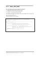
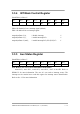
3.3.5 Aux Status Register
(Read/Write): wBase+7
Bit 7 Bit 6 Bit 5 Bit 4 Bit 3 Bit 2 Bit 1 Bit 0
Aux7 Aux6 Aux5 Aux4 Aux3 Aux2 Aux1 Aux0
Note. Refer to Sec. 3.1 for more information about wBase.
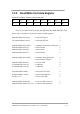
Aux0=PC0, Aux1=PC1, Aux2=PC2, Aux3=PC3, Aux7~4=Aux-ID. Refer to
DEMO5.C for more information. The Aux 0~3 are used as interrupt source. The
interrupt service routine has to read this register for interrupt source identification.
Refer to Sec. 2.5 for more information.
OME-PIO-D56/OME-PIO-D24 User Manual (Ver.2.1, Oct/2003) ---- 35