User's Guide http://www.omega.com e-mail: info@omega.
Table of Contents 1.0 INTRODUCTION .................................................... 1 2.0 INSTALLATION ..................................................... 2.1 HARDWARE INSTALLATION . . . . . . . . . . . . . . . . . . . . . . . . . . . . . . . . . . . . . . . . . 2.2 SOFTWARE INSTALLATION, WINDOWS 95, 98 & NT . . . . . . . . . . . . . . . . . . . . 2.2.1 INTRODUCTION ........................................... 2.2.2 INSTALLATION OPTIONS . . . . . . . . . . . . . . . . . . . . . . . . . . . . . . . .
7.0 PCI-DAS1000 REGISTER DESCRIPTION .............................. 7.1 REGISTER OVERVIEW . . . . . . . . . . . . . . . . . . . . . . . . . . . . . . . . . . . . . . . . . . . . . . 7.2 BADR0 . . . . . . . . . . . . . . . . . . . . . . . . . . . . . . . . . . . . . . . . . . . . . . . . . . . . . . . . . . . . 7.3 BADR1 . . . . . . . . . . . . . . . . . . . . . . . . . . . . . . . . . . . . . . . . . . . . . . . . . . . . . . . . . . . 7.3.1 INTERRUPT / ADC FIFO REGISTER . . . . . . . . . . . . . . . . . .
1.0 INTRODUCTION The PCI-DAS1002 and PCI-DAS1001 are multifunction analog and digital I/O boards designed to operate in computers with PCI bus accessory slots. The boards provide 16 single-ended/8 differential analog inputs with sample rates as high as 150 KHz. The boards also provide two analog output channels, 24-bits of parallel digital I/O and three counters. The only difference between the boards are the analog input ranges. These are shown below. PCI-DAS1002 Bipolar: +/- 10V, 5V, 2.5V and 1.
2.0 INSTALLATION 2.1 HARDWARE INSTALLATION The PCI-DAS1001 and PCI-DAS1002 products are completely plug and play. Simply follow the steps shown below to install your PCI hardware. 1. Turn your computer off, unplug it, open it up and insert the PCI board into any available PCI slot. 2. Close your computer up, plug it back in and turn it on. 3. Windows will automatically detect the board as it starts up. If the board's configuration file is already on the system, it will load without user interaction.
2.3 RUN InstaCal Run the InstaCal program in order to test your board and configure it for run-time use. By configuring the board, you add information to the configuration file, cb.cfg, that is used by the Universal Library and other third-party data acquisition packages that use the Universal Library to access the board. 2.3.1 LAUNCHING InstaCAL Launch InstaCal by going to your Start Menu then to Programs, then to ComputerBoards, and finally choosing InstaCal.
3.0 HARDWARE CONNECTIONS 3.1 CONNECTOR PIN DIAGRAM The PCI-DAS1000 series employ a 100 pin I/O connector. Please make accurate notes and pay careful attention to wire connections. In a large system a misplaced wire may create hours of work ‘fixing’ problems that do not exist before the wiring error is found.
4.0 ANALOG CONNECTIONS 4.1 ANALOG INPUTS Analog signal connection is one of the most challenging aspects of applying a data acquisition board. If you are an Analog Electrical Engineer then this section is not for you, but if you are like most PC data acquisition users, the best way to connect your analog inputs may not be obvious.
Differential Inputs Differential inputs measure the voltage between two distinct input signals. Within a certain range (referred to as the common mode range), the measurement is almost independent of signal source to PCI-DAS1000 ground variations. A differential input is also much more immune to EMI than a single-ended one. Most EMI noise induced in one lead is also induced in the other, the input only measures the difference between the two leads, and the EMI common to both is ignored.
+13V Gray area represents com m on m ode range Both V+ and V- m ust alw ays rem ain w ithin the com m on m ode range relative to LL Gnd +12V +11V +10V +9V +8V +7V W ith Vcm = +5VD C, +Vs m ust be less than +5V, or the com m on m ode range will be exceeded (>+10V) +6V Vcm +5V +4V +3V +2V +1V -1V -2V -3V -4V -5V -6V -7V -8V -9V -10V -11V -12V Vcm (C om m on M ode Voltage) = +5 Volts -13V 4.1.
WARNING If either the AC or DC voltage is greater than 10 volts, do not connect the PCI-DAS1000 to this signal source. You are beyond the boards usable common mode range and will need to either adjust your grounding system or add special Isolation signal conditioning to take useful measurements. A ground offset voltage of more than 30 volts will likely damage the PCI-DAS1000 board and possibly your computer.
Relying on the earth prong of a 120VAC for signal ground connections is not advised.. Different ground plugs may have large and potentially even dangerous voltage differentials. Remember that the ground pins on 120VAC outlets on different sides of the room may only be connected in the basement.
4.2.1 Common Ground / Single-Ended Inputs Single-ended is the recommended configuration for common ground connections. However, if some of your inputs are common ground and some are not, we recommend you use the differential mode. There is no performance penalty (other than loss of channels) for using a differential input to measure a common ground signal source. However the reverse is not true.
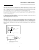
4.2.4 Common Mode Voltage < +/-10V / Differential Inputs Systems with varying ground potentials should always be monitored in the differential mode. Care is required to assure that the sum of the input signal and the ground differential (referred to as the common mode voltage) does not exceed the common mode range of the A/D board (+/-10V on the PCI-DAS1000). The diagram below show recommended connections in this configuration.
Isolatio n B arrie r com m on L a rg e d e vo lta g e n a l mo e e n s ig b o a rd b e tw rc e & A /D so u GND C H H igh + Inp ut Amp To A /D - C H L ow 10 K LL G N D W hen the voltage difference betw een signal source and A /D board gro und is large enough so the A /D board’s com m on m ode ran ge is exceeded, isolated sig nal conditioning m ust be added. I/O C o nn e cto r A /D B oard 1 0K is a reco m m e nd e d v a lu e.
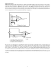
e l S o u rc a rd S ig n a n d A /D B o o la te d . a y Is A lr e a d GND C H H igh + Inp ut Amp C H L ow To A /D - 10 K LL G N D I/O C o nn ec tor T he se g ro u n ds are e lec trica lly isolated . A /D B o a rd 1 0 K is a rec o m m e nd e d v a lue . Yo u m ay s ho rt LL G N D to C H L ow in s te a d , b ut this w ill re du c e yo ur s y s tem ’s n o ise im m u nity. A lready isolated signal source and A /D b oard connected to a differential in pu t.
5.0 PROGRAMMING & SOFTWARE APPLICATIONS Your PCI-DAS1000 is supported by the powerful Universal Library. We strongly recommend that you take advantage of the Universal Library as you software interface. The complexity of the the registers required for automatic calibration combined with the PCI BIOS's dynamic allocation of addresses and internal resources makes the PCI-DAS1000 series very challenging to program via direct register I/O operations.
6.0 SELF-CALIBRATION OF THE PCI-DAS1000 The PCI-DAS1000 is shipped fully-calibrated from the factory with cal coefficients stored in nvRAM. At run time, these calibration factors are loaded into system memory and are automatically retrieved each time a different DAC/ADC range is specified. The user has the option to recalibrate with respect to the factory-measured voltage standards at any time by simply selecting the "Calibrate" option in InstaCal.
6.1.2 Analog Outputs The calibration scheme for the Analog Out section is shown in Figure 2 below.
7.0 PCI-DAS1000 REGISTER DESCRIPTION 7.1 REGISTER OVERVIEW PCI-DAS1000 operation registers are mapped into I/O address space. Unlike ISA bus designs, this board has several base addresses each corresponding to a reserved block of addresses in I/O space. As we mention in our programming chapter, we highly recommend customers use the Universal Library package. Direct register level programming should be attempted only by extremely experienced register level programmers.
INT[1:0] General Interrupt Source selection bits. INT1 INT0 Source 0 0 Not Defined 0 1 End of Channel Scan 1 0 AD FIFO Half Full 1 1 AD FIFO Not Empty INTE Enables interrupt source selected via the INT[1:0] bits. 1 = Selected interrupt Enabled 0 = Selected interrupt Disabled EOAIE Enables End-of-Acquisition interrupt. Used during FIFO'd ADC operations to indicate that the desired sample size has been gathered.
ADHFI Status bit of ADC FIFO Half-Full interrupt. Used during REP INSW operations. 1 = Indicates an ADC Half-Full interrupt has been latched. FIFO has been filled with more than 255 samples. 0 = Indicates an ADC Half-Full interrupt has not occurred. FIFO has not yet exceeded 1/2 of its total capacity. ADNEI Status bit of ADC FIFO Not-Empty interrupt. Used to indicate ADC conversion complete in single conversion applications.
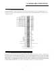
The following tables summarizes all possible Offset/Range configurations: PCI-DAS1002 UNIBIP GS1 GS0 Input Range Input Gain Measurement Resolution 0 0 0 ±10V 1 4.88 mV 0 0 1 ± 5V 2 2.44 mV 0 1 0 ±2.5V 4 1.22 mV 0 1 1 ±1.25V 8 610 uV 1 0 0 0-10V 1 2.44 mV 1 0 1 0-5V 2 1.22 mV 1 1 0 0-2.5V 4 610 uV 1 1 1 0-1.25V 8 305 uV PCI-DAS1001 UNIBIP GS1 GS0 Input Range Input Gain Measurement Resolution 0 0 0 ±10V 1 4.
7.3.3 TRIGGER CONTROL/STATUS REGISTER BADR1 + 4 This register provides control bits for all ADC trigger modes. A Read/Write register.
The table below provides a summary of bit settings and operation. PRTRG FFM0 0 0 0 1 1 0 1 C0SRC ARM is set... FIFO Mode Sample CTR Starts on...
7.3.4 CALIBRATION REGISTER See "Calibrating The PCI-DAS1000" document for additional programming details. BADR1 + 6 This register controls all autocal operations. This is a Write-only register.
7.3.5 DAC CONTROL/STATUS REGISTER BADR1 + 8 This register selects the DAC gain/range and update modes. This is a Write-only register. WRITE 15 14 - - DACEN 13 12 11 10 9 8 7 6 5 4 3 2 1 0 - - DAC1R1 DAC1R0 DAC0R1 DAC0R0 MODE - - - - - DACEN - This bit enables the Analog Out features of the board. 1 = DAC0/1 enabled. 0 = DAC0/1 disabled. The power-on state of this bit is 0. MODE This bit determines the analog output mode of operation.
7.4 BADR2 The I/O Region defined by BADR2 contains the ADC Data register and the ADC FIFO clear register. 7.4.1 ADC DATA REGISTER BADR2 + 0 ADC Data register. WRITE Writing to this register is only valid for SW initiated conversions. The ADC Pacer source must be set to 00 via the ADPS[1:0] bits. A null write to BADR2 + 0 will begin a single conversion. Conversion status may be determined in two ways.
7.5 BADR3 The I/O Region defined by BADR3 contains data and control registers for the ADC Pacer, Pre/Post-Trigger Counters, User Counters and Digital I/O bytes. The PCI-DAS1000 has two 8254 counter/timer devices.
8254A COUNTER 2 DATA - ADC PACER DIVIDER UPPER BADR3 + 2 7 6 D7 D6 READ/WRITE 5 4 D5 D4 2 3 1 0 D3 D2 D1 D0 Counter 1 provides the lower 16 bits of the 32-bit pacer clock divider. Its output is fed to the clock input of Counter 2 which provides the upper 16-bits of the pacer clock divider. The clock input to Counter 1 is a precision 10MHz oscillator source. Counter 2 output is called the 'Internal Pacer' and can be selected by software to the be the ADC Pacer source.
DIO PORT C DATA BADR3 + 6 PORT C may be configured as an 8-bit port of either input or output, or it may be split into two independent 4-bit ports of input or output. When split into two 4-bit I/O ports, D[3:0] make up the lower nibble, D[7:4] comprise the upper nibble. Although it may be split, every write to Port C is a byte operation. Unwanted information must be ANDed out during reads and writes must be ORd with current value of the other 4-bit port.
7.5.3 INDEX and USER COUNTER 4 DATA AND CONTROL REGISTERS 8254B COUNTER 0 DATA - ADC PRE-TRIGGER INDEX COUNTER(or user counter 4) BADR3 + 8 READ/WRITE 7 6 5 4 2 3 1 0 D7 D6 D5 D4 D3 D2 D1 D0 Counter 0 of the 8254B device is a shared resource on the PCI-DAS1000. When not in ADC pre-trigger mode, the clock, gate and output lines of Counter 0 are available to the user at the 100 pin connector as user counter 4. The 8254's Counter 0 clock source is SW selectable via the C0SRC bit in BADR1+4.
8254B CONTROL REGISTER BADR3 + Bh WRITE ONLY 7 D7 6 5 4 2 3 1 0 D6 D5 D4 D3 D2 D1 D0 The control register is used to set the operating Modes of 8254B Counters 0,1 & 2. A counter is configured by writing the correct Mode information to the Control Register, then the proper count data must be written to the specific Counter Register. The Counters on the 8254 are 16-bit devices.
7.6 BADR4 The I/O Region defined by BADR4 contains the DAC0 and DAC1 data registers. 7.6.1 DAC0 DATA REGISTER BADR4 + 0 WRITE 15 14 - - 13 12 - - 11 10 9 DAC0(11) DAC0(10) DAC0(9) 8 7 6 5 4 3 2 1 0 DAC0(8) DAC0(7) DAC0(6) DAC0(5) DAC0(4) DAC0(3) DAC0(2) DAC0(1) DAC0(0) MSB LSB Writing to this register will initiate data conversion on DAC0.
8.0 ELECTRICAL SPECIFICATIONS (Typical specifications for 25 DegC unless otherwise specified.) 8.1 ANALOG INPUT SECTION A/D converter type Resolution Programmable ranges PCI-DAS1001 PCI-DAS1002 A/D pacing Burstmode A/D Trigger sources A/D Triggering Modes Digital: Pre-trigger: 7800 12 bits ±10V, ±1V, ±0.1V, ±0.01V, 0 - 10V, 0 - 1V, 0 - 0.1V, 0 - 0.01V ±10V, ±5V, ±2.5V, ±1.0V, 0 - 10V, 0 - 5V, 0 - 2.5V, 0 - 1.
8.2 ANALOG OUTPUT D/A type Resolution Number of channels Output Ranges AD7847AR 12 bits 2 ±10V, ±5V, 0-5V, 0-10V. Each channel independently programmable. D/A pacing Data transfer Software Programmed I/O. Offset error Gain error Differential nonlinearity Integral nonlinearity Monotonicity D/A Gain drift D/A Bipolar offset drift D/A Unipolar offset drift ±600µV max, all ranges (calibrated) ±0.
8.4 COUNTER SECTION Counter type Configuration 82C54 Two 82C54 devices. 3 down counters per 82C54, 16 bits each 82C54A: Counter 0 - ADC residual sample counter. Source: ADC Clock. Gate: Internal programmable source. Output: End-of-Acquisition interrupt. Counter 1 - ADC Pacer Lower Divider Source: 10 MHz oscillator Gate: Tied to Counter 2 gate, programmable source. Output: Chained to Counter 2 Clock. Counter 2 - ADC Pacer Upper Divider Source: Counter 1 Output.
EC Declaration of Conformity PCI-DAS1000 Part Number High speed analog I/O board for the PCI bus Description to which this declaration relates, meets the essential requirements, is in conformity with, and CE marking has been applied according to the relevant EC Directives listed below using the relevant section of the following EC standards and other normative documents: EU EMC Directive 89/336/EEC: Essential requirements relating to electromagnetic compatibility.