MSP430-5438STK development board Users Manual All boards produced by Olimex are ROHS compliant Rev.
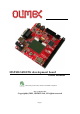
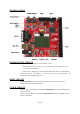
INTRODUCTION MSP430-5438STK development board provides easy way for developing and prototyping with MSP430F5438 mixed signal microcontroller produced by Texas Instruments. This powerful microcontroller supports various serial interfaces such as USB Device, UART, SPI. In addition you will find also audio input and output, debug interface, LCD, UEXT, two Extensions, mini SD/MMC, User Joystick, User Leds, Reset button.
ELECTROSTATIC WARNING The MSP430-5438STK board is shipped in protective anti-static packaging. The board must not be subject to high electrostatic potentials. General practice for working with static sensitive devices should be applied when working with this board. BOARD USE REQUIREMENTS Cables: The cable you will need depends on the programmer/debugger you use. If you use MSP430-JTAG, you will need LPT cable, if you use MSP430-JTAG-TINY or MSP-JTAG-ISO, you will need 1.
– – Fully Integrated LDO With Programmable Regulated Core Supply Voltage – Supply Voltage Supervision, Monitoring, and Brownout Unified Clock System – FLL Control Loop for Frequency Stabilization – Low-Power/Low-Frequency Internal Clock Source (VLO) – Low-Frequency Trimmed Internal Reference Source (REFO) – 32-kHz Crystals – High-Frequency Crystals up to 32 MHz – 16-Bit Timer TA0, Timer_A With Five Capture/Compare Registers – 16-Bit Timer TA1, Timer_A With Three Capture/Compare Registers
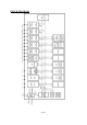
BLOCK DIAGRAM Page 5
MEMORY ORGANIZATION Page 6
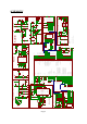
USB NA C48 NA C43 100nF C44+ 10uF/6.3V/T ANT Page 7 P_OUT HN1x2 2 1 2 1 #LCD_RES EXT1-28 A_OUT 67 66 65 61 60 59 58 57 MSP430F5438IPZ P8.7 P8.6/TA1.1 P8.5/TA1.0 P8.4/TA0.4 P8.3/TA0.3 P8.2/TA0.2 P8.1/TA0.1 P8.0/TA0.0 P7.7/A15 P7.6/A14 P7.5/A13 P7.4/A12 P7.3/TA1.2 P7.2/TB0OUTH/SVMOUT P7.1/XOUT P7.0/XIN P6.7/A7 P6.6/A6 P6.5/A5 P6.4/A4 P6.3/A3 P6.2/A2 P6.1/A1 P6.0/A0 P5.7/UCA1RXD/UCA1SOMI P5.6/UCA1TXD/UCA1SIMO P5.5/UCB1CLK/UCA1STE P5.4/UCB1SOMI/UCB1SCL P5.3/XT2OUT P5.2/XT2IN P5.
BOARD LAYOUT POWER SUPPLY CIRCUIT MSP430-5438STK can take power from three sources: – PWR connector where 9 V DC or 6 V AC is applied by external power source. – +5V_USB from USB DEV – JTAG, when P_IN jumper is closed. Note that the JTAG has current limitations. The board power consumption is: about 20 mA with all peripherals and microcontroller running at full speed. RESET CIRCUIT MSP430-5438STK reset circuit includes JTAG connector pin 11, EXT1 pin 3, MSP430F5438 pin 96 and Reset button.
JUMPER DESCRIPTION Power In jumper: P_IN jumper connects power supply from JTAG connector. You have to ensure that your circuit doesn't draw more than few milliampers current or the power supply may decrease due to the JTAG port current limitations. P_IN is useful and must be used mostly to program the microcontroller. Power Out jumper: P_OUT jumper connects power from MSP430-5438STK to JTAG connector.
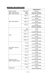
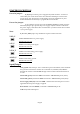
CONNECTOR DESCRIPTIONS JTAG Pin # Signal Name Pin # Signal Name 1 TDO 2 VCC_IN 3 TDI 4 VCC_OUT 5 TMS 6 NC 7 TCK 8 TEST 9 GND 10 NC 11 #RST 12 NC 13 NC 14 NC RS232 Pin # Signal Name 1 NC 2 PC_RXD 3 PC_TXD 4 PC_DTR 5 GND 6 PC_DSR 7 PC_RTS 8 PC_CTS 9 NC Page 10
USB DEV Pin # Signal Name 1 +5V_USB 2 USBDM 3 USBDP 4 GND PWR_JACK Pin # Signal Name 1 Power Input 2 GND UEXT Pin # Signal Name 1 3.
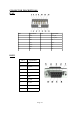
EXT1 Pin # Signal Name Pin # Signal Name 1 3.3V 2 GND 3 #RST 4 TCK 5 TMS 6 TDI 7 TDO 8 P11.2 9 P11.1 10 P11.0 11 LED1 12 LED2 13 UCA3RXD 14 UCA3TXD 15 P10.3 16 P10.2 17 P10.1 18 P10.0 19 UCB2CLK 20 UCB2SOMI 21 UCB2SIMO 22 P8.7 23 P8.6 24 P8.5 25 P8.4 26 P8.3 27 P8.2 28 P8.0 29 P7.2 30 P7.3 31 P7.4 32 P7.5 33 P7.6 34 P7.
EXT2 Pin # Signal Name Pin # Signal Name 1 3.3VA 2 AGND 3 P1.7 4 P1.1 5 P1.0 6 P2.7 7 P2.6 8 P2.5 9 P2.4 10 P2.3 11 P2.2 12 P2.1 13 P2.0 14 UCB0CLK 15 UCB0SOMI 16 UCB0SIMO 17 UCB0STE 18 P4.7 19 P4.6 20 P4.5 21 P4.4 22 P4.3 23 P4.2 24 P4.1 25 P4.0 26 P6.6 27 P6.5 28 P6.4 29 P6.3 30 P6.2 31 P6.1 32 P6.0 33 P5.0 34 P5.
SD/MMC Pin # Signal Name 1 Pull-up 2 UCB0STE 3 UCB0SIMO 4 VDD (power supply) 5 UCB0CLK 6 GND 7 UCB0SOMI 8 Pull-up 9 Not connected 10 Not connected 11 Not connected 12 Not connected Microphone Pin # Signal Name 1 AGND 2 NC 3 MIC Headphone Pin # Signal Name 1 AGND 2 IN1=IN2 3 IN2=IN1 Page 14
MECHANICAL DIMENSIONS Page 15
AVAILABLE DEMO SOFTWARE – Display demo – LEDs and Buttons demo – SD/MMC demo – UART demo – USB UART demo – ADC and DAC demo Page 16
ORDER CODE MSP430-5438STK – assembled and tested (no kit, no soldering required) How to order? You can order to us directly or by any of our distributors. Check our web www.olimex.com/dev for more info. Revision history: REV.A - October 2009 Initial release REV.
Disclaimer © 2009 Olimex Ltd. All rights reserved. Olimex®, logo and combinations thereof, are registered trademarks of Olimex Ltd. Other terms and product names may be trademarks of others. The information in this document is provided in connection with Olimex products. No license, express or implied or otherwise, to any intellectual property right is granted by this document or in connection with the sale of Olimex products.