E2E1027-27-Y4 This version: Jan. 1998 MSM66201/66P201/66207/66P207 Previous version: Nov. 1996 ¡ Semiconductor MSM66201/66P201/66207/ 66P207 ¡ Semiconductor OLMS-66K Series 16-Bit Microcontroller GENERAL DESCRIPTION The MSM66201/66207 is a high performance microcontroller that employs OKI original nX-8/ 200 CPU core. This chip includes a 16-bit CPU, ROM, RAM, I/O ports, multifunction 16-bit timers, 10-bit A/D converter, serial I/O port, and pulse width modulator (PWM).
¡ Semiconductor MSM66201/66P201/66207/66P207 • Package 64-pin plastic shrink DIP (SDIP64-P-750-1.78) * : (MSM66201-¥¥¥SS) (MSM66P201-¥¥¥SS) (MSM66207-¥¥¥SS) (MSM66P207-¥¥¥SS) 64-pin plastic QFP (QFP64-P-1414-0.80-BK) : (MSM66201-¥¥¥GSBK)(MSM66207¥¥¥GSBK) 68-pin plastic QFJ (PLCC) (QFJ68-P-S950-1.27) : (MSM66201-¥¥¥JS) (MSM66P201-¥¥¥JS) (MSM66207-¥¥¥JS) (MSM66P207-¥¥¥JS) 64-pin ceramic piggyback (ADIP64-C-750-1.78) : (MSM66G207VS) (¥¥¥ indicates the code number.
INTERRUPT CONT. PERIPHERAL CONT. NMI P3.2/INT0 P3.3/INT1 P2.3/CLKOUT RESOUT WDT PWM 0,1 P4.2/PWM0 P4.3/PWM1 A/D CONV. TRANSITION D. SERIAL PORT TIMER 0–3 CONT. SYSTEM CONTROLLER ACCUMULATOR TEMPORARY R. CONSTANTS ALU ALU SSP PSW INSTRUCTION DECODER LRB PC RAP IR CONT. MEMORY PORT ROM 32K ¥ 8 bits *1 RAM 1024 ¥ 8 bits *2 A15/P1.7 A8 /P1.0 AD7/P0.7 AD0/P0.0 WR RD PSEN ALE READY EA *1 MSM66201 16K ¥ 8 *2 MSM66201 512 ¥ 8 C O N T . P O R T B U S BLOCK DIAGRAM P5.
¡ Semiconductor MSM66201/66P201/66207/66P207 PIN CONFIGURATION (TOP VIEW) AD0/P0.0 1 64 VDD AD1/P0.1 2 63 VREF AD2/P0.2 3 62 AGND AD3/P0.3 4 61 P5.7/AI7 AD4/P0.4 5 60 P5.6/AI6 AD5/P0.5 6 59 P5.5/AI5 AD6/P0.6 7 58 P5.4/AI4 AD7/P0.7 8 57 P5.3/AI3 A8/P1.0 9 56 P5.2/AI2 A9/P1.1 A10/P1.2 10 11 55 54 P5.1/AI1 P5.0/AI0 A11/P1.3 12 53 P4.7/TRNS3 A12/P1.4 13 52 P4.6/TRNS2 A13/P1.5 14 51 P4.5/TRNS1 A14/P1.6 15 50 P4.4/TRNS0 A15/P1.7 16 49 P4.3/PWM1 P2.
, ¡ Semiconductor MSM66201/66P201/66207/66P207 49 P5.3/AI3 50 P5.4/AI4 54 P5.5/AI5 52 P5.6/AI6 53 P5.7/AI7 54 AGND 55 VREF 56 VDD 57 P0.0/AD0 58 P0.1/AD1 59 P0.2/AD2 60 P0.3/AD3 61 P0.4/AD4 62 P0.5/AD5 63 P0.6/AD6 64 P0.7/AD7 PIN CONFIGURATION (TOP VIEW) (Continued) 1 48 P5.2/AI2 2 47 P5.1/AI1 3 46 P5.0/AI0 4 45 P4.7/TRNS3 5 44 P4.6/TRNS2 6 43 P4.5/TRNS1 7 42 P4.4/TRNS0 8 41 P4.3/PWM1 9 40 P4.2/PWM0 P2.1 10 39 P4.1/TM1CK P2.2 11 38 P4.0/TM0CK CLKOUT/P2.3 12 37 P3.
¡ Semiconductor MSM66201/66P201/66207/66P207 44 P3.3/INT1 46 P3.5/TM1IO 45 P3.4/TM0IO 48 P3.7/TM3IO 47 P3.6/TM2IO 50 P4.0/TM0CK 49 NC 52 P4.2/PWM0 51 P4.1/TM1CK 54 P4.4/TRNS0 53 P4.3/PWM1 56 P4.6/TRNS2 55 P4.5/TRNS1 58 P5.0/AI0 57 P4.7/TRNS3 60 P5.2/AI2 59 P5.1/AI1 PIN CONFIGURATION (TOP VIEW) (Continued) AI3/P5.3 61 AI4/P5.4 62 43 P3.2/INT0 42 P3.1/RXD AI5/P5.5 63 AI6/P5.6 64 41 P3.0/TXD 40 P2.7/RXC AI7/P5.7 65 AGND 66 39 P2.6/TXC 38 P2.5/HLDA VREF 67 VDD 68 37 P2.
¡ Semiconductor MSM66201/66P201/66207/66P207 PIN DESCRIPTION Symbol Type Description P0.0–P0.7/ AD0–AD7 I/O P0: 8-bit input-output port. Each bit can be assigned to input or output. AD: Outputs the lower 8 bits of program counter during external program memory fetch, and receives the addressed instruction under the control of PSEN. This pin also outputs the address and outputs or inputs data during an external data memory access instruction, under the control of ALE, RD, and WR. P1.0–P1.
¡ Semiconductor MSM66201/66P201/66207/66P207 PIN DESCRIPTION (Continued) Symbol Type Description RESOUT O Outputs "H" level in the case of internal reset. Reset to"L" level by program. ALE O Address Latch Enable: The timing pulse to latch the lower 8 bits of the address output from port 0 when the CPU accesses the external memory. PSEN O Program Strobe Enable: The strobe pulse to fetch to external program memory. RD O WR O READY I Output strobe activated during a bus read cycle.
¡ Semiconductor MSM66201/66P201/66207/66P207 REGISTERS Accumulator 15 0 ACC Control Register (CR) 15 0 PSW Bit 15 : Carry flag (CY) Bit 14 : Zero flag (ZF) Bit 13 : Half carry flag (HC) Bit 12 : Data descriptor (DD) Bit 8 : Master interrupt priority flag (MIP) Bit 9,5,4: User flag (MIP) Bit 2-0 : System control base 2-0 (SCB2-0) 15 0 PC LRB SSP Pointing Register (PR) 15 0 Index Register 1 X1 Index Register 2 X2 Data Pointer DP USP User Stack Pointer Local Register 7 0 7 0 ER0 R1 R0 ER1
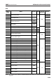
¡ Semiconductor MSM66201/66P201/66207/66P207 SFR Address (HEX) 0000 0001 0002 0003 0004I 0005I 0006 0007 0010I Name Symbol R/W SSP (ASSP) FFH Local register base LRB (ALRB) undefined Program status word Accumulator Standby control register PSWL (APSW) FFH R/W 00H ACC 00H SBYCON F8H 00H/WDT is stopped WDT W Peripheral control register PRPHF R/W 0013 Stop code acceptor STPACP W 001A 001B 8 FDH "0" 00H IRQ 8/16 Interrupt enable register C8H 0CH Watchdog timer Interrupt reque
¡ Semiconductor MSM66201/66P201/66207/66P207 SFR (Continued) Addres (HEX) 0038 0039 003A 003B 003C Name Abbreviated Name Timer 2 counter TM2 Timer 2 register TMR2 R/W 8/16-bit Operation Reset 00H 00H 00H 16 00H 00H Timer 3 counter TM3 Timer 3 register TMR3 0040 Timer 0 control register TCON0 0041 Timer 1 control register TCON1 0042 Timer 2 control register TCON2 0043 Timer 3 control register TCON3 00H 0046I TRNSIT undefined 0048 Transition detector register Serial port tra
¡ Semiconductor MSM66201/66P201/66207/66P207 SFR (Continued) Address (HEX) 0062I 0063 0064I 0065 0066I 0067 0068I Name Abbreviated Name A/D conversion result register 1 ADCR1 A/D conversion result register 2 ADCR2 A/D conversion result register 3 ADCR3 ADCR4 A/D conversion result register 5 ADCR5 A/D conversion result register 6 ADCR6 A/D conversion result register 7 ADCR7 PWM 0 counter PWMC0 PWM 0 register PWMR0 PWM 1 counter PWMC1 PWM 1 register PWMR1 0078 PWM 0 control register
¡ Semiconductor MSM66201/66P201/66207/66P207 ADDRESSING MODES The MSM66201/66207 provides independent 64K-byte data and 64K-byte program space with various types of addressing modes. These modes are shown below, for both RAM (for data space) and ROM (for program space). 1. RAM Addressing Modes (for data space) 1.1 Register Direct Addressing Example ROR DP DP 1.2 Displacement Addressing a) Zero Page Example L A, 18H SFR 0000H 0018H b) Direct Page Example ST A, off 10H RAM xx00H xx10H 1.
¡ Semiconductor MSM66201/66P201/66207/66P207 c) Index Register (X1, X2) Indirect Example INC 300H [X1] RAM X1 0 to 65535 1.4 Immediate Addressing Example MOV SSP, #27FH 2. ROM Addressing Modes (for program space) 2.1 Direct Addressing Example LC A, 200H ROM 0200H 2.
¡ Semiconductor 3) MSM66201/66P201/66207/66P207 Index Register (X1, X2) Indirect Example LC A, [X1] ROM X1 c) System Stack Pointer (SSP) Indirect Example LC A, [SSP] ROM SSP d) Local Register Base (LRB) Indirect Example LC A, [LRB] ROM LRB e) RAM Indirect Example J A, [0C0H] RAM 2.
¡ Semiconductor MSM66201/66P201/66207/66P207 c) Index Register (X1, X2) Double Indirect Example LC A, [10000H [x1]] RAM X1 ROM 0 to 65535 2.
¡ Semiconductor MSM66201/66P201/66207/66P207 MEMORY MAPS Program Memory Space 0000H 0000H 0027H 0028H Internal ROM Area 0037H 0038H Vector Table Area (40 bytes) VCAL Table Area (16 bytes) 7FFFH * External Memory FFFFH 7FFFH * * MSM66201 : 3FFFH Data Memory Space Zero Page 0000H 007FH 0080H 00BFH 00C0H 00FFH 0100H 0000H SFR Area Special Function Registors PR Area PORT, A/DC, TIMER, PWM, etc....
¡ Semiconductor MSM66201/66P201/66207/66P207 ABSOLUTE MAXIMUM RATINGS (Ta=25°C) Parameter Supply Voltage Condition Symbol Rating Input Voltage VI –0.3 to VDD+0.3 Output Voltage VO –0.3 to VDD+0.3 GND=AGND=0V Analog Ref. Voltage VREF –0.3 to VDD+0.3 Analog Input Voltage VAI –0.3 to VREF 64-pin shrink DIP Power Dissipation Storage Temperature PD Unit –0.3 to 7.
¡ Semiconductor MSM66201/66P201/66207/66P207 ELECTRICAL CHARACTERISTICS DC Characteristics Parameter "H" Input Voltage 1, 3, 6 "H" Input Voltage 5, 7 (VDD = 5V ± 10%, Ta = –40 to +85°C) Symbol Condition VIH — Min. 2.4 Typ. — Max. VDD+0.3 4.0 — VDD+0.3 Unit 4.2 — VDD+0.3 "H" Input Voltage 2 3.6 — VDD+0.3 "L" Input Voltage 1, 2, 3, 6 –0.3 — 0.8 –0.3 — 0.8 –0.3 — 0.4 IO = –400mA 4.2 — — IO = –200mA 4.2 — — IO = 3.2mA — — 0.4 IO = 1.6mA — — 0.
¡ Semiconductor MSM66201/66P201/66207/66P207 AC Characteristics • External program memory control Symbol Condition Clock (OSC) Pulse Parameter tfW — ALE Pulse Width PSEN Pulse Width (VDD=5V±10%, Ta=–40 to +85°C) Min. Max.
¡ Semiconductor MSM66201/66P201/66207/66P207 CLK t∆W t∆W ALE tAW PSEN tPAD AD0-7 tPW PC0-7 INST0-7 tAAS tAAH A8-15 tIS tIH PC8-15 tAAD tAPH RD tRAD AD0-7 tRW RAP0-7 tAAS DIN 0-7 tAAH A8-15 tMS tMH RAP8-15 tAAD tAPH WR tWAD AD0-7 tWW RAP0-7 tAAS A8-15 DOUT0-7 tAAH tDD tDH RAP8-15 tAAD tAWH 21/30
¡ Semiconductor MSM66201/66P201/66207/66P207 • Serial port control Master mode (VDD=5V±10%, Ta=–40 to +85°C) Parameter Symbol Condition Min. Max. Clock (OSC) Pulse Width tfW — 50 — — Serial Clock Pulse Width tSCKW 8tfW — Output Data Setup Time tSTMXS 8tfW+40 — Output Data Hold Time tSTMXH 6tfW–20 — Input Data Setup Time tSRMXS 2tfW+10 — Input Data Hold Time tSRMXH 50 — CL=50pF Slave mode Unit ns (VDD=5V±10%, Ta=–40 to +85°C) Parameter Symbol Condition Min. Max.
1 0 / .
¡ Semiconductor MSM66201/66P201/66207/66P207 A/D Converter Characteristics • Operating range Parameter Symbol Condition Min. Typ. Max. VDD fOSC £ 10MHz 4.5 — 5.5 Power Supply Voltage Analog Reference Voltage VR 4.
¡ Semiconductor MSM66201/66P201/66207/66P207 • Recommended circuit Reference Voltage VREF +5V VDD + 0.1 47 mF mF RI – + + 0.1 47 mF mF AI0-7 ~ GND Analog Input 0V AGND 0.
¡ Semiconductor MSM66201/66P201/66207/66P207 Absolute error (EA) The absolute error indicates a difference between actual conversion and ideal conversion, excluding a quantizing error. The absolute error of the A/D converter gets larger as it approaches the zero point or full scale. (Refer to Conversion Characteristics Diagram 1.
¡ Semiconductor MSM66201/66P201/66207/66P207 PACKAGE DIMENSIONS (Unit : mm) SDIP64-P-750-1.78 Package material Lead frame material Pin treatment Solder plate thickness Package weight (g) Epoxy resin Cu alloy Solder plating 5 mm or more 8.70 TYP. Notes for Mounting the Surface Mount Type Package The SOP, QFP, TSOP, SOJ, QFJ (PLCC), SHP and BGA are surface mount type packages, which are very susceptible to heat in reflow mounting and humidity absorbed in storage.
¡ Semiconductor MSM66201/66P201/66207/66P207 (Unit : mm) QFP64-P-1414-0.80-BK Mirror finish Package material Lead frame material Pin treatment Solder plate thickness Package weight (g) Epoxy resin 42 alloy Solder plating 5 mm or more 0.87 TYP. Notes for Mounting the Surface Mount Type Package The SOP, QFP, TSOP, SOJ, QFJ (PLCC), SHP and BGA are surface mount type packages, which are very susceptible to heat in reflow mounting and humidity absorbed in storage.
¡ Semiconductor MSM66201/66P201/66207/66P207 (Unit : mm) QFJ68-P-S950-1.27 Mirror finish Package material Lead frame material Pin treatment Solder plate thickness Package weight (g) Epoxy resin Cu alloy Solder plating 5 mm or more 4.50 TYP. Notes for Mounting the Surface Mount Type Package The SOP, QFP, TSOP, SOJ, QFJ (PLCC), SHP and BGA are surface mount type packages, which are very susceptible to heat in reflow mounting and humidity absorbed in storage.
¡ Semiconductor MSM66201/66P201/66207/66P207 (Unit : mm) ADIP64-C-750-1.78 Notes for Mounting the Surface Mount Type Package The SOP, QFP, TSOP, SOJ, QFJ (PLCC), SHP and BGA are surface mount type packages, which are very susceptible to heat in reflow mounting and humidity absorbed in storage.
This datasheet has been download from: www.datasheetcatalog.com Datasheets for electronics components.