
Datasheet


UBA2028 All information provided in this document is subject to legal disclaimers. © NXP B.V. 2010. All rights reserved.
Product data sheet Rev. 02 — 19 July 2010 6 of 23
NXP Semiconductors
UBA2028
600 V dimmable power IC for compact fluorescent lamps
8. Functional description
8.1 Start-up state
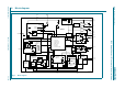
Initial start-up can be achieved by charging the low voltage supply capacitor at pin 16 (see
Figure 8
and Figure 9) via an external start-up resistor. Start-up of the circuit is achieved
under the condition that both half-bridge transistors TR1 and TR2 are non-conductive.
The circuit will be reset in the start-up state. If the low voltage supply (V
DD
) reaches the
value of V
DD(startup)
the circuit will start oscillating. A DC reset circuit is incorporated in the
High-Side (HS) driver. Below the lockout voltage at the FS pin the output voltage (TR1
gate voltage − V
SH
) is zero. The voltages at pins CF and CT are zero during the start-up
state.
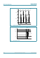
8.2 Oscillation
The internal oscillator is a Voltage Controlled Oscillator (VCO) circuit which generates a
sawtooth waveform between the V
o(osc)max
level and 0 V. The frequency of the sawtooth is
determined by capacitor C
CF
, resistor R
IREF
, and the voltage at pin CSW. The minimum
and maximum switching frequencies are determined by R
IREF
and C
CF
; their ratio is
internally fixed. The sawtooth frequency is twice the half-bridge frequency. The UBA2028
brings the transistors TR1 and TR2 into conduction alternately with a duty cycle of
approximately 50 %. An overview of the oscillator signal and driver signals is illustrated in
Figure 7
. The oscillator starts oscillating at f
max
. During the first switching cycle the
Low-Side (LS) transistor (TR2) is switched on. The first conducting time is made extra
long to enable the bootstrap capacitor to charge.
8.3 Adaptive non-overlap
The non-overlap time is realized with an adaptive non-overlap timing circuit (ANT). By
using an adaptive non-overlap circuit, the application can determine the duration of the
non-overlap time and make it optimum for each frequency; see Figure 7
. The non-overlap
time is determined by the slope of the half-bridge voltage, and is detected by the signal
across resistor R15 see Figure 8
(R6 in Figure 9) which is connected directly to pin ACM.
The minimum non-overlap time is internally fixed. The maximum non-overlap time is
internally fixed at approximately 25 % of the bridge period time. An internal filter of 30 ns
is included at the ACM pin to increase the noise immunity.
8.4 Timing circuit
A timing circuit is included to determine the preheat time and the ignition time. The circuit
consists of a clock generator and a counter.
The preheat time is defined by C
CT
and R
IREF
connected to pins 10 and 13, and consists
of 7 pulses at C
CT
; the maximum ignition time is 1 pulse at C
CT
. The timing circuit starts
operating after the start-up state, as soon as the low supply voltage (V
DD
) has reached
V
DD(startup)
or when a critical value of the lamp voltage (V
lamp(fail)
) is exceeded. When the
timer is not operating C
CT
is discharged to 0 V at 1 mA.