
Datasheet


UBA2028 All information provided in this document is subject to legal disclaimers. © NXP B.V. 2010. All rights reserved.
Product data sheet Rev. 02 — 19 July 2010 14 of 23
NXP Semiconductors
UBA2028
600 V dimmable power IC for compact fluorescent lamps
V
O(osc)max
maximum oscillator output
voltage
f=f
min
-2.5-V
I
o(startup)
start-up output current for oscillator; V
CF
= 1.5 V 3.8 4.5 5.2 μA
I
osc
oscillator current V
CF
=1.5V 21 - 54 μA
Output driver
Low-side driver output: pin GLO
V
OH
HIGH-level output voltage I
o
=10mA 12.5--V
V
OL
LOW-level output voltage I
o
=10mA - - 0.5 V
I
O(source)
output source current V
GLO
= 0 V 135 180 235 mA
I
sink(o)
output sink current V
GLO
= 13 V 265 330 415 mA
R
on
on-state resistance I
o
=10mA 32 39 45 Ω
R
off
off-state resistance I
o
=10mA 16 21 26 Ω
Output stage
Power transistors
R
on
on-state resistance TR1 high-side power - - 3 Ω
TR2 low-side power - - 3 Ω
R
on(150)
/R
on(25)
on-state resistance ratio
(150 °Cto25°C)
-2.7--
Floating supply voltage: pin FS
V
FS
voltage on pin FS for lockout 2.8 3.5 4.2 V
I
FS
current on pin FS DC level at TR1 gate
voltage − V
SH
=13V
-35-μA
Bootstrap diode
V
Fd(bs)
bootstrap diode forward voltage I = 5 mA 1.3 1.7 2.1 V
Preheat current sensor
Input: pin PCS
I
I
input current V
i(PCS)
=0.6V - - 1 μA
V
ph
preheat voltage 0.57 0.60 0.63 V
Output: pin CSW
I
source(o)
output source current V
i(CSW)
= 2.0 V 9.0 10 11 μA
I
sink(o)
output sink current V
i(CSW)
=2.0V - 10 - μA
Adaptive non-overlap and capacitive mode detection; pin ACM
I
I
input current V
i(ACM)
=0.6V - - 1 μA
V
det(capm)
capacitive mode detection
voltage
positive 80 100 120 mV
negative −68 −85 −102 mV
Input: pin LVS
I
I
input current V
i(LVS)
=0.81V - - 1 μA
V
lamp(fail)
lamp fail voltage 0.77 0.81 0.85 V
V
lamp(fail)hys
lamp fail voltage hysteresis 119 144 169 mV
V
lamp(max)
maximum lamp voltage 1.44 1.49 1.54 V
Table 6. Characteristics
…continued
V
DD
=13V; V
FS
−
V
SH
=13V; T
amb
=25
°
C; all voltages referenced to GND unless otherwise specified
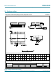
(see application circuits of Figure 8 and Figure 9).
Symbol Parameter Conditions Min Typ Max Unit