
Datasheet


TJA1028 All information provided in this document is subject to legal disclaimers. © NXP B.V. 2012. All rights reserved.
Product data sheet Rev. 4 — 25 July 2012 12 of 24
NXP Semiconductors
TJA1028
LIN transceiver with integrated voltage regulator
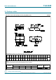
[1] See Figure 1 and Figure 6.
[2] Not tested in production; guaranteed by design.
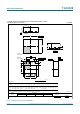
[3] See Figure 8
.
V
BUSrec
receiver recessive state V
BAT
= 5.5 V to 18 V 0.6
V
BAT
--V
V
BUSdom
receiver dominant state V
BAT
= 5.5 V to 18 V - - 0.4
V
BAT
V
V
BUS_CNT
receiver center voltage V
BAT
= 5.5 V to 18 V;
V
BUS_CNT
= (V
BUSdom
+ V
BUSrec
)/2
[3]
0.475
V
BAT
0.5
V
BAT
0.525
V
BAT
V
V
HYS
receiver hysteresis voltage V
BAT
= 5.5 V to 18 V;
V
HYS
= V
BUSrec
V
BUSdom
[3]
0.05
V
BAT
0.15
V
BAT
0.175
V
BAT
V
V
SerDiode
voltage drop at the serial
diode
in pull-up path with R
slave
;
I
SerDiode
=0.9mA
[2]
0.4 - 1.0 V
C
LIN
capacitance on pin LIN with respect to GND
[2]
- - 30 pF
V
O(dom)
dominant output voltage Normal mode;
V
TXD
= 0 V; V
BAT
= 7 V
--1.4V
Normal mode;
V
TXD
= 0 V; V
BAT
= 18 V
--2.0V
R
slave
slave resistance between pin LIN and V
BAT
;
V
LIN
=0 V; V
BAT
=12V
20 30 60 k
Temperature protection
T
th(act)otp
overtemperature protection
activation threshold
temperature
165 180 195 C
T
th(rel)otp
overtemperature protection
release threshold
temperature
126 138 150 C
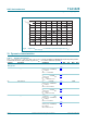
Table 6. Static characteristics …continued
V
BAT
= 5.5 V to 28 V; T
vj
=
40
C to +150
C; R
L(LIN-VBAT)
= 500
; all voltages are defined with respect to ground; positive
currents flow into the IC; typical values are given at V
BAT
= 12 V; unless otherwise specified.
Symbol Parameter Conditions Min Typ Max Unit