
Datasheet

TEF6901A_3 © NXP B.V. 2008. All rights reserved.
Product data sheet Rev. 03 — 20 March 2008 77 of 107
NXP Semiconductors
TEF6901A
Integrated car radio
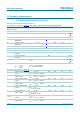
I
sink(CP5)
charge pump CP5 sink
current
V
CPOUT
= 0.7 V to
V
CCPLL
− 0.7 V; f
ref
= 10 kHz
1630 2 200 2970 µA
I
source(CP5)
charge pump CP5
source current
V
CPOUT
= 0.7 V to
V
CCPLL
− 0.7 V; f
ref
= 10 kHz
−2970 −2200 −1630 µA
Charge pump: pin VTUNE
I
sink
charge pump sink
current
V
VTUNE
= 0.8 V to
V
CCPLL
− 0.7 V
2070 2800 3780 µA
I
source
charge pump source
current
V
VTUNE
= 0.8 V to
V
CCPLL
− 0.7 V
−3780 −2800 −2070 µA
t
tune
tuning time Europe FM and US FM band;
f
ref
= 100 kHz; f
RF
= 87.5 MHz
to 108 MHz
- 0.75 1 ms
AM MW band; f
ref
= 20 kHz;
f
RF
= 0.53 MHz to 1.7 MHz
- 5 20 ms
T
cy
inaudible AF update
cycle time including
1 ms mute start and
1 ms mute release time
- 6 6.5 ms
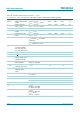
Antenna Digital Auto Alignment (DAA)
DAA: pin DAAOUT
[2]
I
leak(DAA)
antenna DAA input
leakage current on pin
VTUNE (test mode)
V
VTUNE
= 0.4 V to 8 V −10 - +10 nA
∆V
o(T)
output voltage variation
with temperature
T
amb
= −40 °C to +85 °C;
DAA[6:0] = 100 0000
−30 - +30 mV
∆V
o(sink)
output voltage variation
caused by sink current
V
VTUNE
=4V; I
L
=50µA −V
LSB
-+V
LSB
∆V
o(source)
output voltage variation
caused by source
current
V
VTUNE
=4V; I
L
= −50 µA −V
LSB
-+V
LSB
t
st
settling time V
DAAOUT
= 0.2 V to 8.25 V;
C
L
= 270 pF
-3060 µs
AM mode
V
o
output voltage DAA[6:0] = 000 0000 - - 0.5 V
DAA[6:0] = 111 1111 8.0 - 8.5 V
FM mode
V
o(n)
output noise voltage V
VTUNE
=4V;
DAA[6:0] = 100 0000;
B = 300 Hz to 22 kHz
- 30 100 µV
RR ripple rejection V
VTUNE
=4V;
DAA[6:0] = 101 0101;
f
ripple
= 100 Hz;
V
CC(ripple)
= 100 mV
-40- dB
∆V
o(step)
step accuracy V
VTUNE
=2V −0.5V
LSB
0 +0.5V
LSB
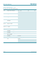
Table 110. Dynamic characteristics of the tuner
…continued
V
CC
= 8.5 V; T
amb
=25
°
C; see Figure 43; all AC values are given in RMS; unless otherwise specified.
Symbol Parameter Conditions Min Typ Max Unit