
Datasheet

TEF6901A_3 © NXP B.V. 2008. All rights reserved.
Product data sheet Rev. 03 — 20 March 2008 73 of 107
NXP Semiconductors
TEF6901A
Integrated car radio
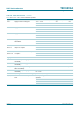
8.2.28 Write mode: data byte TEST
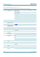
9. Limiting values
[1] The maximum voltage should be less than 10 V.
[2] Class 2 according to JESD22-A114D.
[3] Class B according to EIA/JESD22-A115-A.
[4] Class 1C according to JESD22-A114D.
[5] Class A according to EIA/JESD22-A115-A.
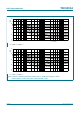
Table 105. TEST - format of data byte 1Fh
7 6 5 4 3 2 1 0
RBWR 0 TEST5 TEST4 TEST3 TEST2 TEST1 TEST0
0 000000
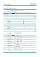
Table 106. TEST - data byte 1Fh bit description
Bit Symbol Description
7 RBWR next I
2
C-bus read contains write register data (RBWR will be reset to logic 0 after read)
6 - reserved; 0 = normal operation
5 to 0 TEST[5:0] test mode
00 0000 = normal operation
00 1011 = AM IF noise blanker disabled
00 1110 = AM IF noise blanker disabled
01 1001 = AM audio noise blanker and FM noise blanker disabled
all other settings are reserved
Table 107. Limiting values
In accordance with the Absolute Maximum Rating System (IEC 60134).
Symbol Parameter Conditions Min Max Unit
V
CC
analog supply voltage on pins VCC,
VCCPLL, VCCVCO, VCCRF,
AMMIX2OUT1, AMMIX2OUT2, MIX1OUT1
and MIX1OUT2
−0.3 +10 V
∆V
CC
voltage difference between any VCC pins −0.3 +0.3 V
V
V60
supply voltage for FM filter and demodulator
[1]
−0.3 V
CC
+ 0.3 V
V
I
digital input voltage on pins SCL, SDA and
ADDR
−0.3 +5.5 V
V
n
voltage on all other pins
[1]
−0.3 V
CC
+ 0.3 V
T
stg
storage temperature −40 +150 °C
T
j
junction temperature - 150 °C
T
amb
ambient temperature −40 +85 °C
V
esd
electrostatic discharge voltage on
all pins except VCCVCO human body model
[2]
−2000 +2000 V
machine model
[3]
−200 +200 V
pin VCCVCO human body model
[4]
−1750 +1750 V
machine model
[5]
−175 +175 V