
Datasheet


NXP Semiconductors
UM10973
LPCXpresso54114
UM10973
All information provided in this document is subject to legal disclaimers.
© NXP B.V. 2016. All rights reserved.
User manual
Rev. 1.1 — 25 February 2016
7 of 21
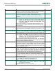
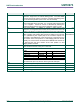
Circuit ref
Description
Ref section
P1
10-pin SWD connector – The SWD connector is used to debug the
LPC54114 Target from an external debug probe. The same SWD
connector can also be used to connect the on-board Link2 debug probe
to an off-board target MCU (for this JP1 must be shunted).
6
P2
LPC54114 VDD current monitor Vsense measurement. The Vsense
can be measured with a volt meter. Pin 1 (square pad) is positive and
pin 2 is negative. LPC54114 current is calculated by dividing the
measured voltage at P2 by the Vsense resistance value of 4.12Ω.
5.1.1
P3
FTDI serial header. In addition to provide a serial output from
LPC54114, the Target side of the board can be powered from the FTDI
header. The LPC54114 supports serial ISP boot from the FTDI header.
4.1
P4
External ADC reference input. The pads of this header enable external
VREF (negative and positive) ADC reference voltages to be injected.
Pin 1 (indicated by the square pad) of the connector footprint can
connected to the VREFP pin of the LPC54114 by removing the zero
ohm resistor at SJ2 from position 1-2 and bridging pads 2-3 instead.
Similarly, Pin 3 of P4 can be connected to the VREFN of the LPC54114
by removing the zero ohm resistor at SJ1 from position 1-2 and
bridging pads 2-3 instead.
LPC54110
User Manual
SW1
LPC54114 Target WAKE pushbutton. When pressed the WAKE
switch will drive LPC54114 P0_24 to a low level.
9.3
SW2, SW3
These switches can be used to force the LPC54114 in to ISP boot
modes:
Boot mode
ISP0
ISP1
Vbus (from J5)
I2C/SPI boot
Pressed
Pressed
X
UART boot
Pressed
0
USB Mass storage
Pressed
1
Boot from internal flash
After reset these pins may also be used to generate interrupts.
9.2
SW4
LPC54114 Target Reset pushbutton.
9.1
TP1
Ground terminal test point.
n/a
U12
Link2 MCU
n/a
U11
LPC54114 Target LQFP64 MCU
n/a